 2
2
PNY RTX 4060 Ti XLR8 Review
Test Setup »High-resolution PCB Pictures
These pictures are for the convenience of volt modders and people who would like to see all the finer details on the PCB. Feel free to link back to us and use these in your articles, videos or forum posts.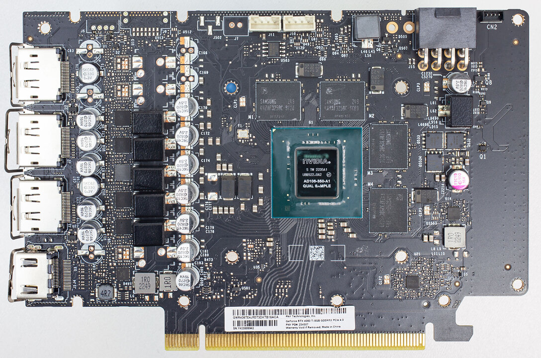
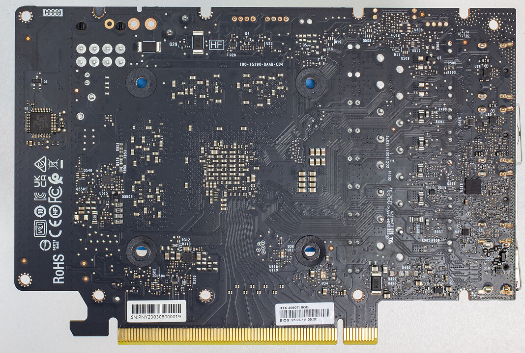
High-resolution versions are also available (front, back).
Circuit Board (PCB) Analysis
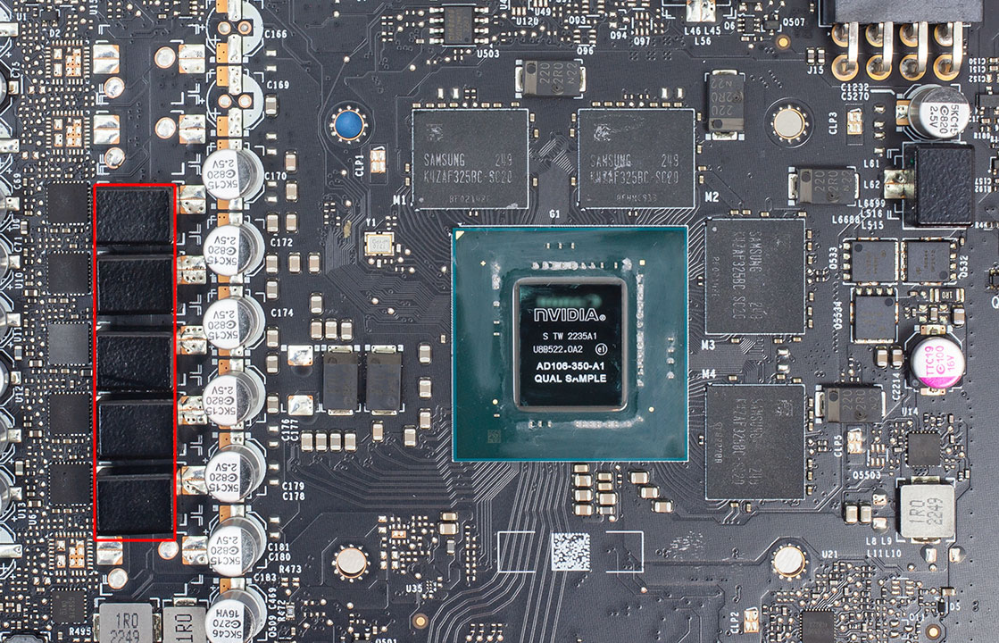
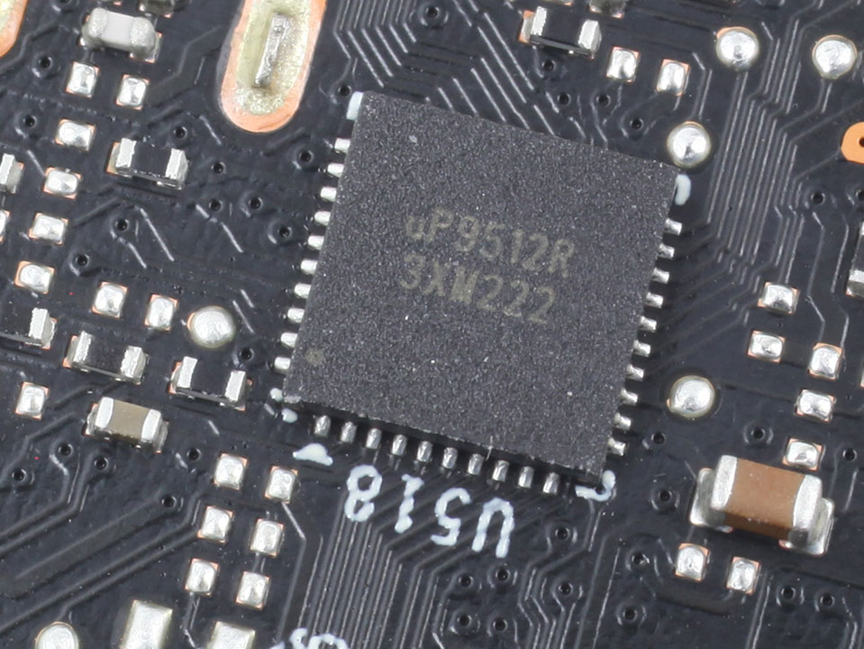
The PNY XLR8 appears to be using the same exact PCB as the RTX 4060 Ti Verto we reviewed earlier, the only change is the more premium memory chips. The GPU voltage is taken care of by a 5-phase design, with a UPI uP9512R controller in charge.
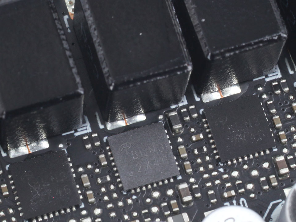
Alpha & Omega AOZ5311NQI BLN3 DrMOS components are used for GPU voltage; they are rated for 55 A of current each.
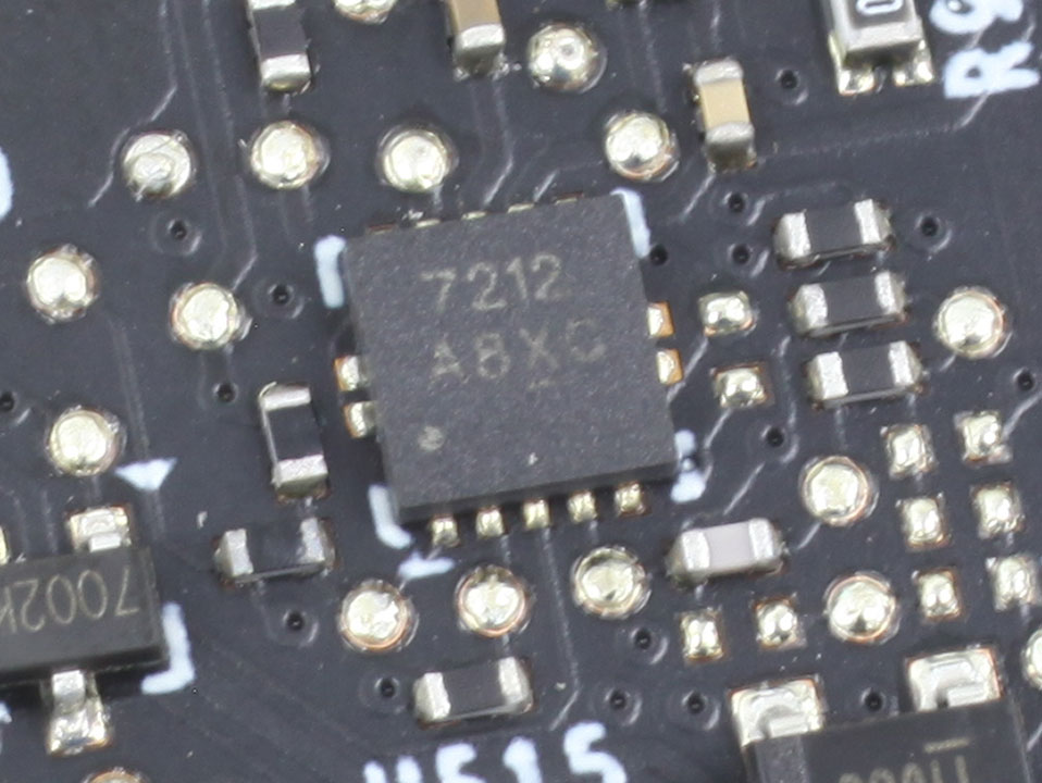
Memory voltage is a single-phase design, managed by a 7212 buck controller.
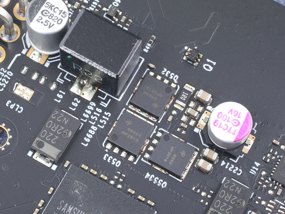
For memory, Alpha and Omega 36344 discrete MOSFETs are used.
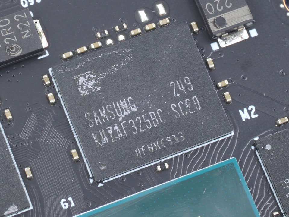
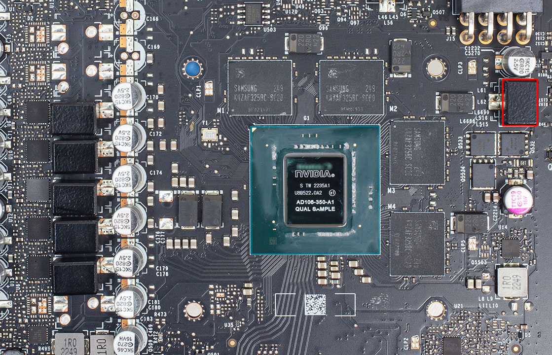
The memory chips are Samsung K4ZAF325BC-SC20, these are 20 Gbps-rated GDDR6 memory chips.
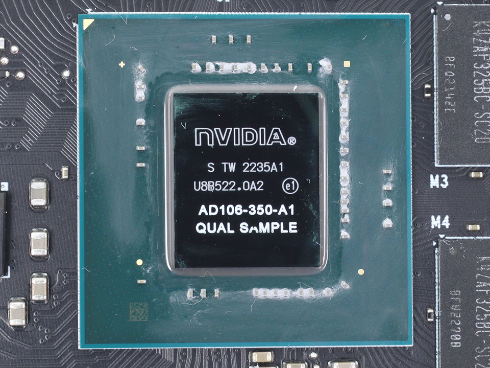
NVIDIA's AD106 graphics processor is the company's fourth Ada Lovelace GPU. It is built using a 5 nanometer process at TSMC Taiwan, with a transistor count of 22.9 billion and a die size of 190 mm².
Feb 7th, 2025 18:57 EST
change timezone
Latest GPU Drivers
New Forum Posts
- WCG Daily Numbers (12756)
- Official TECHPOWERUP HWBOT Team Information Thread (33)
- RTX5000 Series Owners Club (59)
- Folding Pie and Milestones!! (9362)
- What's your latest tech purchase? (23108)
- should global c-state be "enabled" instead of auto on am5 x3d processors? (8)
- 5090 OC Insanity? (1)
- RTX 3060 i5-10400 32gb ram become very slow after cleaning (5)
- Which is your favourite controller? (77)
- TOXIC AMD Radeon™ RX 6900 XT (58)
Popular Reviews
- Kingdom Come Deliverance II Performance Benchmark Review - 35 GPUs Tested
- Spider-Man 2 Performance Benchmark Review - 35 GPUs Tested
- Corsair Frame 4000D Review
- Formovie Cinema Edge 4K UST Laser Projector Review
- ASUS ROG Harpe Ace Extreme Review
- Kingdom Come: Deliverance 2 Handheld Performance Review
- NVIDIA GeForce RTX 5080 Founders Edition Review
- AMD Ryzen 7 9800X3D Review - The Best Gaming Processor
- Gigabyte GeForce RTX 5080 Gaming OC Review
- MSI GeForce RTX 5080 Vanguard SOC Review
Controversial News Posts
- AMD Radeon 9070 XT Rumored to Outpace RTX 5070 Ti by Almost 15% (286)
- AMD is Taking Time with Radeon RX 9000 to Optimize Software and FSR 4 (256)
- AMD Denies Radeon RX 9070 XT $899 USD Starting Price Point Rumors (239)
- Edward Snowden Lashes Out at NVIDIA Over GeForce RTX 50 Pricing And Value (235)
- AMD Radeon RX 9070 XT & RX 9070 Custom Models In Stock at European Stores (226)
- New Leak Reveals NVIDIA RTX 5080 Is Slower Than RTX 4090 (215)
- AMD's Radeon RX 9070 Launch Faces Pricing Hurdles (175)
- AMD Radeon RX 9070 XT Tested in Cyberpunk 2077 and Black Myth: Wukong (169)