 103
103
AMD Radeon RX 6600 Review - Great for 1080p Gaming
Test Setup »High-resolution PCB Pictures
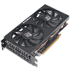
These pictures are for the convenience of volt modders and people who would like to see all the finer details on the PCB. Feel free to link back to us and use these in your articles, videos or forum posts.High-res versions are also available (front, back).
Circuit Board (PCB) Analysis
GPU voltage uses a 6-phase design and is powered by an IR35217 controller.
The GPU VRM uses OnSemi NCP302155 DrMOS components rated for 55 A.
Memory voltage uses a two-phase design and is generated by an NCP81022N controller.
For memory, 45 A OnSemi DrMOS components are used.
The GDDR6 memory chips are made by Hynix! First time we encounter Hynix GDDR6 memory in a TPU graphics card review. The model number is H56CBM24MIR-S2C. They are specified to run at 1750 MHz (14 Gbps GDDR6 effective).
Built on the same TSMC N7 (7 nm) node as Navi 10, the Navi 23 silicon is spread across a 237 mm² die area and packs 11.6 billion transistors. The pinkish-red tinge we saw on Navi 10 is gone.
Jan 24th, 2025 15:24 EST
change timezone
Latest GPU Drivers
New Forum Posts
- Post your Speedtest.net Speeds! (2338)
- NVidia now HIDING hot spot temperature? A great problem IMO. (59)
- Testing max ram overclock pn Ryzen 1700 (7)
- Any information about RTX 5090 performance at 5K-8K? (3)
- RANT- front panel connectors are a crime against pc builders/users (49)
- Undervolting vs Power Limiting (4)
- Anime Nation (12964)
- Fractal define R4 vs R5 build quality. (24)
- [SOLVED] Frametime spikes/Stutters/FPS drops in all games. (287)
- The coffee and tea appreciation thread (162)
Popular Reviews
- NVIDIA GeForce RTX 5090 Founders Edition Review - The New Flagship
- NVIDIA GeForce RTX 5090 Founders Edition Unboxing
- NVIDIA GeForce RTX 5090 PCI-Express Scaling
- ASUS GeForce RTX 5090 Astral OC Review - Astronomical Premium
- MSI GeForce RTX 5090 Suprim SOC Review
- MSI GeForce RTX 5090 Suprim Liquid SOC Review
- Alphacool Apex 1 CPU Water Block Review - Performance King!
- Pwnage StormBreaker Max CF Review
- NZXT C1500 Review
- PowerColor Alphyn AH10 Review
Controversial News Posts
- NVIDIA 2025 International CES Keynote: Liveblog (470)
- AMD Debuts Radeon RX 9070 XT and RX 9070 Powered by RDNA 4, and FSR 4 (349)
- AMD is Taking Time with Radeon RX 9000 to Optimize Software and FSR 4 (237)
- AMD Radeon RX 9070 XT & RX 9070 Custom Models In Stock at European Stores (226)
- NVIDIA GeForce RTX 5090 Features 575 W TDP, RTX 5080 Carries 360 W TDP (217)
- AMD's Radeon RX 9070 Launch Faces Pricing Hurdles (175)
- Potential RTX 5090 and RTX 5080 Pricing in China Leaks (173)
- AMD Radeon RX 9070 XT Tested in Cyberpunk 2077 and Black Myth: Wukong (169)


