 39
39
Sapphire Radeon RX 5500 XT Pulse 4 GB Review
Test Setup »High-resolution PCB Pictures
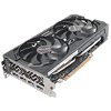
These pictures are for the convenience of volt modders and people who would like to see all the finer details on the PCB. Feel free to link back to us and use these in your articles or forum posts.High-res versions are also available (front, back).
Circuit Board (PCB) Analysis
The GPU VRM is a staggering 6-phase setup controlled by an International Rectifier IR35217 controller mated with LFPAK MOSFETs.
The memory VRM is single-phase and managed by an OnSemi NCP81022N controller (another premium part that's originally designed for 4 phases).
The GDDR6 memory chips are made by Micron and carry the model number D9WCW, which decodes to MT61K256M32JE-14:A. They are specified to run at 1750 MHz (14 Gbps GDDR6 effective).
AMD's Navi 14 graphics processor is their second chip to use the new RDNA graphics architecture. It is made on a 7 nanometer silicon fabrication process at TSMC and has a transistor count of 6.4 billion. The die measures just 158 mm².
Feb 20th, 2025 22:00 EST
change timezone
Latest GPU Drivers
New Forum Posts
- [PCGamer] Former Sony exec finally says the quiet part out loud: putting PlayStation games on PC is 'almost like printing money' (22)
- Will undervolting a 4090 keep the connector from melting? A discussion about electrical theory. (15)
- DDR3 voltage question. (16)
- Project 2004, a retro time capsule (90)
- First ever PC build (6)
- [LPC Project] - DARK KNIGHT II (5)
- Stalker 2 is looking great. (165)
- It's happening again, melting 12v high pwr connectors (840)
- AIO - 120mm cpu cooler? (25)
- RTX 5090 ridiculous price! (178)
Popular Reviews
- MSI GeForce RTX 5070 Ti Ventus 3X OC Review
- Gigabyte GeForce RTX 5090 Gaming OC Review
- Galax GeForce RTX 5070 Ti 1-Click OC White Review
- Ducky One X Inductive Keyboard Review
- ASUS GeForce RTX 5070 Ti TUF OC Review
- MSI GeForce RTX 5070 Ti Vanguard SOC Review
- AMD Ryzen 7 9800X3D Review - The Best Gaming Processor
- MSI MAG Z890 Tomahawk Wi-Fi Review
- MSI GeForce RTX 5070 Ti Gaming Trio OC+ Review
- NVIDIA GeForce RTX 5080 Founders Edition Review
Controversial News Posts
- AMD Radeon 9070 XT Rumored to Outpace RTX 5070 Ti by Almost 15% (302)
- AMD is Taking Time with Radeon RX 9000 to Optimize Software and FSR 4 (256)
- AMD Plans Aggressive Price Competition with Radeon RX 9000 Series (255)
- AMD Radeon RX 9070 and 9070 XT Listed On Amazon - One Buyer Snags a Unit (242)
- Edward Snowden Lashes Out at NVIDIA Over GeForce RTX 50 Pricing And Value (241)
- AMD Denies Radeon RX 9070 XT $899 USD Starting Price Point Rumors (239)
- New Leak Reveals NVIDIA RTX 5080 Is Slower Than RTX 4090 (215)
- AMD Radeon RX 9070 XT Launch Allegedly Set for March 6 (152)


