 111
111
Sapphire Radeon RX 7900 XTX Nitro+ Review - Maxing out 3x 8-Pin
(111 Comments) »Introduction
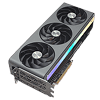
Sapphire NITRO+ Radeon RX 7900 XTX is the company's flagship air-cooled graphics card based on Team Red's fastest next-generation GPU. The NITRO+ brand in its latest generation incorporates a more flamboyant, colorful, and industrial product design, not too unlike the ASUS ROG STRIX. Large ARGB LED diffusers accentuate a premium cooler shroud, with three of Sapphire's latest-generation fans in a cooling solution Sapphire calls the Pantheon+. Each of the three fans can be easily disconnected and individually pulled out of the cooler, the TriXX software can detect faults in each fan, letting you request RMAs easily, in case of issues. The cooler features a new composite material for the heatpipes. Other gamer-friendly features include dual-BIOS, a reinforcement brace, ARGB headers to let you sync the rest of your rig's lighting with the card (controllable through the TriXX software), and a display output setup that includes two each of HDMI 2.1b and DisplayPort 2.1 connectors.
The new AMD Radeon RX 7900 XTX is the top dog graphics card based on AMD's new RDNA 3 graphics architecture. The company has attempted to keep Moore's Law alive in spirit by designing the "Navi 31" silicon powering this graphics card to be the first gaming GPU to incorporate chiplets (a multi-chip module with multiple logic dies that functionally make up a single chip). AMD identified specific components of the GPU that don't benefit from the latest foundry node as much as the pure logic components, such as stream processors; and disintegrated them from the GPU die. The "Navi 31" GPU features six Memory Cache Dies (MCDs), each built on the slightly older 6 nm process. Inside each MCD you'll find a 64-bit GDDR6 memory interface, the memory controller backing it, and a 16 MB segment of the GPU's 96 MB Infinity Cache. Six of these make up the GPU's 384-bit GDDR6 memory interface. The rest of the GPU with the bulk of the pixel-crunching machinery, is nucleated into a large die called the Graphics Compute Die (GCD), built on the 5 nm EUV process. The move helps save costs by maximizing its 5 nm wafer allocation with TSMC, and the company made sure to transfer some of these savings over to customers, with the Radeon RX 7900 series being 20-50% cheaper than the high-end NVIDIA GeForce RTX 40-series "Ada" GPUs launched to date, which are built on monolithic 5 nm dies.

The new RDNA 3 graphics architecture sees the introduction of a new-generation Compute Unit (CU) with dual instruction issue-rate stream processors, support for new math formats, AI acceleration, and 2nd generation Ray Accelerators. There are 96 CUs spread across six Shader Engines, which make up 6,144 stream processors, 96 Ray Accelerators, 384 TMUs, and a whopping 192 ROPs. The RX 7900 XTX maxes out the "Navi 31" silicon enabling all 96 CU available, and the GPU's full 384-bit GDDR6 memory interface. It now enjoys 24 GB of GDDR6 memory ticking at 20 Gbps, which works out to an impressive 960 GB/s memory bandwidth (87% higher than that of the RX 6900 XT), allowing AMD to slightly reduce the size of the Infinity Cache memory.
With RDNA 3, AMD is hoping to repeat the 50% performance/Watt generational gain that springboarded it back to the high-end PC graphics segment with RDNA 2. The 20% higher CU count, each with 17.5% higher IPC over RDNA 2 CUs, coupled with higher engine clocks, and a faster memory sub-system, together help AMD achieve a 53% generational performance/Watt uplift that's needed to remain competitive with NVIDIA. The RX 7900 XTX has a starting MSRP of USD $999, which is 20% cheaper than the NVIDIA RTX 4080, and 60% less than that of the RTX 4090 flagship, while targeting the same market—4K Ultra HD maxed-out gaming with ray tracing.
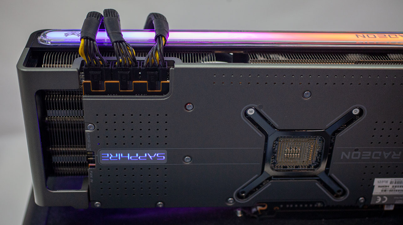
The Sapphire Radeon RX 7900 XTX NITRO+ OC ups the game with not just the various hard-product feature-additions, but also a factory-overclock, with the Game Clock set up to 2510 MHz compared to 2455 MHz reference. As we've seen on other non-reference cards, the RX 7900 XTX truly comes to life with a stronger power delivery system. The NITRO+ draws power from three 8-pin PCIe power connectors, which combined with the PCIe slot power, add up to 525 W. With its primary BIOS, the card has a power-limit of 420 W (compared to 350 W reference), which should enable higher boost frequency residency. The Tri-X Pantheon cooling solution, offers a low noise output. Official pricing hasn't been released yet, but we're expecting a $1100 price point, which makes the card $100 more expensive than the AMD reference design MSRP.
| Price | Cores | ROPs | Core Clock | Boost Clock | Memory Clock | GPU | Transistors | Memory | |
|---|---|---|---|---|---|---|---|---|---|
| RTX 3070 | $500 | 5888 | 96 | 1500 MHz | 1725 MHz | 1750 MHz | GA104 | 17400M | 8 GB, GDDR6, 256-bit |
| RTX 3070 Ti | $600 | 6144 | 96 | 1575 MHz | 1770 MHz | 1188 MHz | GA104 | 17400M | 8 GB, GDDR6X, 256-bit |
| RX 6800 | $510 | 3840 | 96 | 1815 MHz | 2105 MHz | 2000 MHz | Navi 21 | 26800M | 16 GB, GDDR6, 256-bit |
| RX 6800 XT | $650 | 4608 | 128 | 2015 MHz | 2250 MHz | 2000 MHz | Navi 21 | 26800M | 16 GB, GDDR6, 256-bit |
| RTX 3080 | $750 | 8704 | 96 | 1440 MHz | 1710 MHz | 1188 MHz | GA102 | 28000M | 10 GB, GDDR6X, 320-bit |
| RTX 3080 Ti | $950 | 10240 | 112 | 1365 MHz | 1665 MHz | 1188 MHz | GA102 | 28000M | 12 GB, GDDR6X, 384-bit |
| RX 6900 XT | $700 | 5120 | 128 | 2015 MHz | 2250 MHz | 2000 MHz | Navi 21 | 26800M | 16 GB, GDDR6, 256-bit |
| RX 6950 XT | $800 | 5120 | 128 | 2100 MHz | 2310 MHz | 2250 MHz | Navi 21 | 26800M | 16 GB, GDDR6, 256-bit |
| RTX 3090 | $950 | 10496 | 112 | 1395 MHz | 1695 MHz | 1219 MHz | GA102 | 28000M | 24 GB, GDDR6X, 384-bit |
| RX 7900 XT | $900 | 5376 | 192 | 2000 MHz | 2400 MHz | 2500 MHz | Navi 31 | 57700M | 20 GB, GDDR6, 320-bit |
| RTX 3090 Ti | $1400 | 10752 | 112 | 1560 MHz | 1950 MHz | 1313 MHz | GA102 | 28000M | 24 GB, GDDR6X, 384-bit |
| RTX 4080 | $1200 | 9728 | 112 | 2205 MHz | 2505 MHz | 1400 MHz | AD103 | 45900M | 16 GB, GDDR6X, 256-bit |
| RX 7900 XTX | $1000 | 6144 | 192 | 2300 MHz | 2500 MHz | 2500 MHz | Navi 31 | 57700M | 24 GB, GDDR6, 384-bit |
| Sapphire RX 7900 XTX Nitro+ | $1100 | 6144 | 192 | 2510 MHz | 2680 MHz | 2500 MHz | Navi 31 | 57700M | 24 GB, GDDR6, 384-bit |
| RTX 4090 | $2400 | 16384 | 176 | 2235 MHz | 2520 MHz | 1313 MHz | AD102 | 76300M | 24 GB, GDDR6X, 384-bit |
AMD RDNA 3 Graphics Architecture


The Radeon RX 7900 XTX and RX 7900 XT debut AMD's 3rd generation RDNA graphics architecture, termed RDNA 3. With it, AMD plans to repeat the generational 50% performance/Watt gain it achieved with RDNA 2, which sprung it back to the high-end graphics segment after a long gap. AMD claims it succeeded in this endeavor, with a 54% generational performance/Watt gain. At the heart of this effort is the switch to the new TSMC 5 nm EUV foundry node. AMD figured out early on that it cannot build large monolithic GPUs on 5 nm without thinning its margins in the fight against NVIDIA, and set out to innovate the Chiplet architecture for the GPU. Under this, specific parts of the GPU that actually benefit from a switch to a newer foundry node, such as the Shader Engines, would be built on a centralized 5 nm die called the Graphics Compute Die (GCD), while those components that can make do with a less advanced node, namely the memory controllers and L3 cache, would be spun off to chiplets called Memory Cache Dies (MCDs), built on 6 nm.


The "Navi 31" GPU is hence a chiplet GPU and not a multi-chip module like "Vega 10." In a chiplet-based device, various components that can otherwise not exist on their own packages, are placed on a single package, with the goal of minimizing production costs, by stratifying their need for a new foundry node, such that only the most power-intensive IP receive the most advanced node. In a MCM, chips that can otherwise exist on their own package, are combined onto a single package for conserving PCB real-estate, or reducing latency. The GCD in the "Navi 31" GPU hence has all the shader engines, caches up to L2, the front-end Command Processor, Async Compute Engines (ACEs), the Display Engine, and the Media Engine. Each of the six MCDs has a 64-bit wide memory bus, and a 16 MB segment of the GPU's 96 MB Infinity Cache memory. The size of the Infinity Cache may have been generationally reduced (compared to 128 MB on "Navi 21"), but AMD has widened the memory bus itself, from 256-bit up to 384-bit.


Much of the architectural innovation is not with the chiplet design (a packaging innovation); but at the level of the RDNA 3 Dual-Compute Unit (or Compute Unit pair). The "Navi 31" GPU physically features 96 compute units spread across six Shader Engines. AMD claims that at the same engine clocks, the RDNA 3 CU offers a 17.4% IPC increase over the RDNA 2 CU. There are 20% more CUs over the "Navi 21," and these run at higher engine clocks, tapping into the power headroom afforded by the 5 nm process. These combined work out to the 54% generational performance uplift, with which AMD plans to retain competitiveness with NVIDIA's RTX 40-series "Ada" high-end SKUs.


The new RDNA 3 CU introduces multi-precision capability for the 64 stream processors per CU: operating either as 1x SIMD64 or 2x SIMD32 units. The Vector Unit that houses these SIMD units can either function as a SIMD execution mechanism, or as a Matrix execution unit, thanks to the new AI Matrix Accelerator, which provides a 2.7x matrix multiplication performance uplift versus conventional SIMD execution. Also added are support for the Bfloat16 instruction-set, and SIMD8 execution. The GPU hence enjoys AI hardware-acceleration that can be leveraged in future feature-additions relevant to gamers, such as FSR 3.0. Game developers will also look for ways to exploit accelerated AI, now that all three brands feature it (NVIDIA Tensor cores and Intel XMX cores).


AMD's first-generation Ray Accelerator, introduced with the RDNA 2 architecture, was the result of a hasty effort to catch up to NVIDIA with a DirectX 12 Ultimate GPU, where they developed a fixed-function hardware to calculate ray intersections, and offloaded a large chunk of RT processing to the generationally-doubled SIMD resources. With RDNA 3, they've refined the Ray Accelerator to achieve an 80% ray tracing performance uplift over the previous generation, when you add up the Ray Accelerator count, their higher engine clocks, and other hardware-level optimizations, such as early sub-tree culling, specialized box sorting modes, and reduced traversal iterations.


There is a 50% ray intersection capacity improvement for the "Navi 31" GPU thanks to these optimizations, and cycles-per-ray reduction. Besides these, AMD has also made several improvements to the geometry- and pixel-pipes, with the introduction of the new multi-draw indirect accelerator (MDIA), which reduces CPU API and driver-level overheads by gathering and parsing multi-draw command data. At the hardware-level 12 primitives per clock is now supported compared to 8 per clock on RDNA 2, thanks to culling. The core-configuration overall enables 50% more rasterized performance per clock.
The GCD features six Shader Engines, each with 16 compute units (or 8 dual compute units), which work out to 1,024 stream processors. Six such Shader Engines make up 6,144 stream processors with 96 Ray Accelerators and 96 AI Accelerators. The GPU has 384 TMUs, and a massive 192 ROPs—a 50% increase over "Navi 21." The Radeon RX 7900 XTX enables all 96 CUs, and maxes out the silicon, whereas the RX 7900 XT has 84 out of 96 CUs enabled, which work out to 5,376 stream processors, 84 Ray Accelerators, 336 TMUs, and an unchanged 192 ROPs. The RX 7900 XTX gets 24 GB of GDDR6 memory across the GPU's entire 384-bit memory bus, with a memory speed of 20 Gbps (GDDR6-effective), translating to 960 GB/s of memory bandwidth. The RX 7900 XT is equipped with 20 GB of memory across a narrower 320-bit memory bus carved out by disabling one of the six MCDs. At the same 20 Gbps speed, this yields 800 GB/s bandwidth.


AMD has significantly improved the Display Engine of "Navi 31" over the previous-generation in terms of connectivity. The new Radiance Display Engine comes with native support for DisplayPort 2.1, which enables 8K output at up to 165 Hz refresh-rate, or 4K at up to 480 Hz, with a single cable. AMD has refined its FSR 2 algorithm to support 8K (i.e. render at a lower resolution with FSR-enhanced upscaling), to make it possible to enjoy the latest AAA titles at playable frame-rates on 8K displays. Both the RX 7900 series cards get two full-size DP 2.1 connectors, besides an HDMI 2.1b, and a USB-C with DP 1.2 passthrough. The "Navi 31" silicon receives full hardware-accelerated AV1 encode and decode capabilities, through dual independent encode/decoders, so two independent video streams can be simultaneously transcoded, or one stream at twice the framerate. With this generation, AMD is also introducing SmartAccess Video, a feature that lets the AMD driver leverage the hardware encoders of the RDNA 2 iGPU of Ryzen 7000 desktop processors, for additional encoding performance.
Packaging

The Card
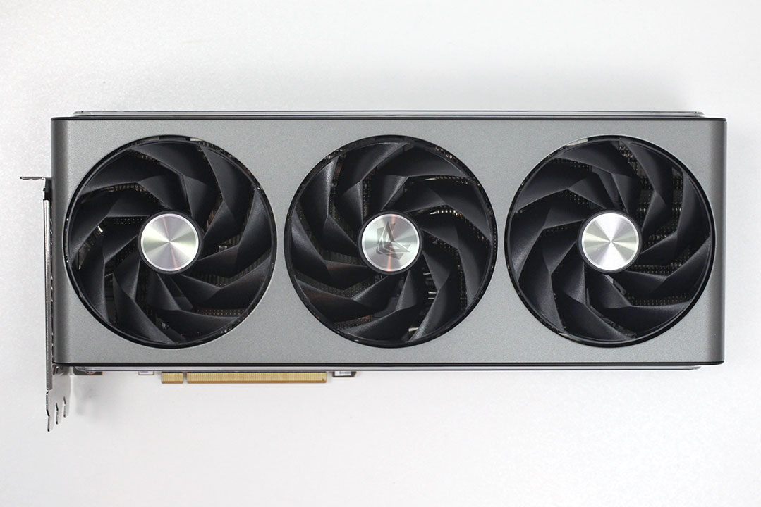
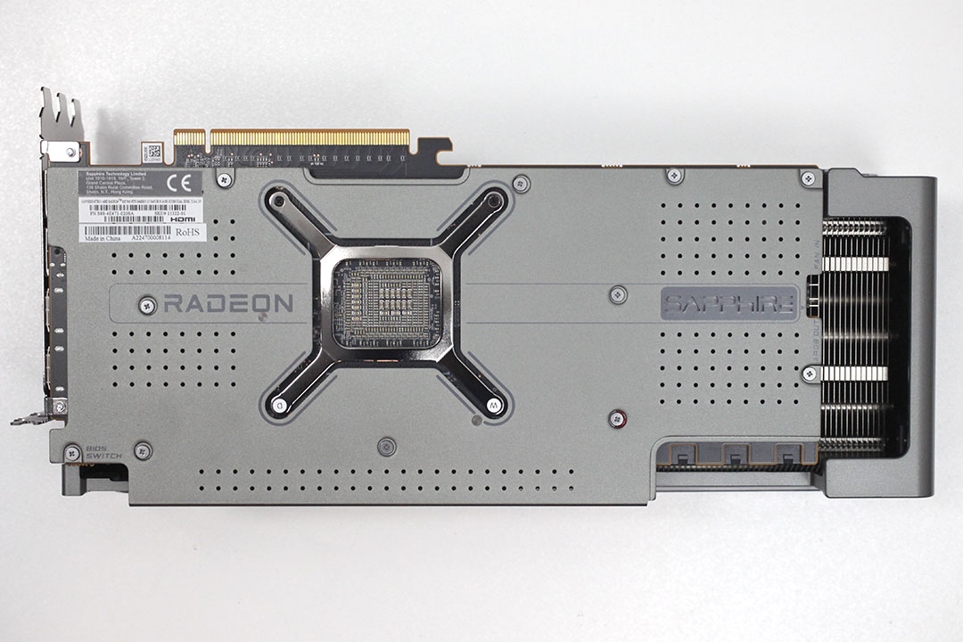
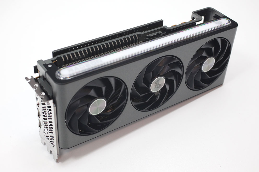
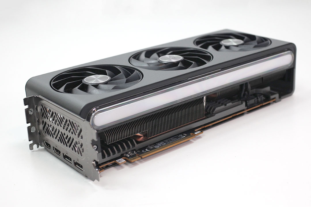
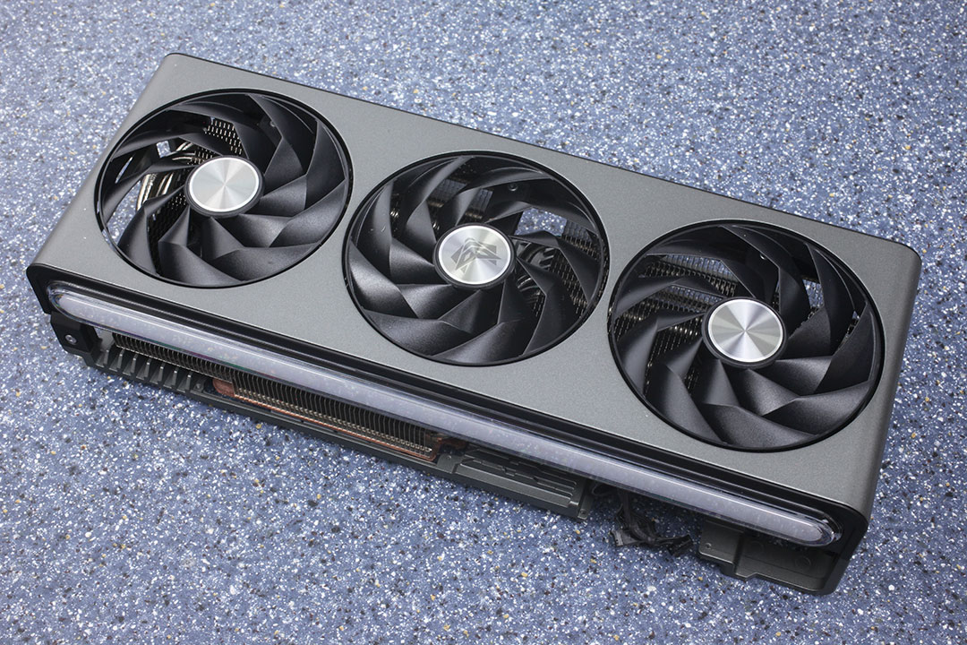
For the new RDNA 3 Radeon RX 7000 Series of graphics cards, Sapphire has come up with a completely new design. The main color is a matte gray that looks stunning. I love the looks of the main cooler, it's almost like it came right out of Apple's design labs. The metal backplate is a bit more busy, with various cutouts, logos and labels.

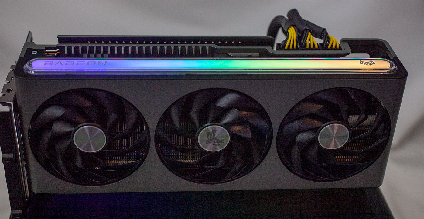
Sapphire has installed an amazing RGB solution on their Nitro+. You get two smooth lighting bars that Sapphire calls "Pantheon+," one on top of the card and one on the bottom. There's an additional RGB-illuminated Sapphire logo on the back.
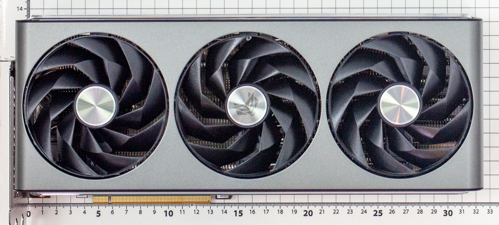
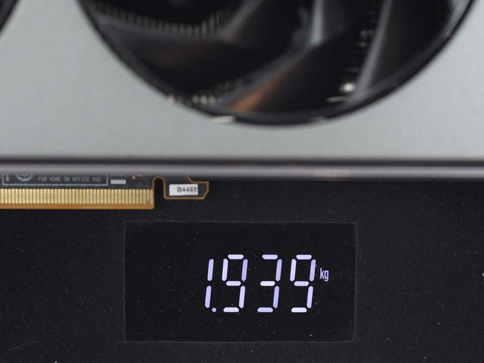
Dimensions of the card are 31.5 x 13.5 cm, and it weighs 1939 g.
Installation requires four slots in your system.
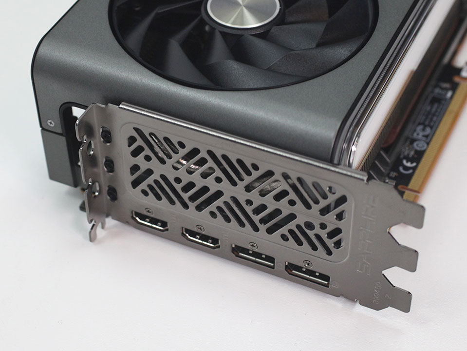
Display connectivity includes two standard DisplayPort 2.1 ports (RDNA 2 had 1.4a) and two HDMI 2.1a (same as RDNA 2).
AMD has upgraded their encode/decode setup. It now comes with two independent hardware units that can encode and decode two streams of video in parallel, or one stream at double the FPS rate. There's support for VP9, H.264, H.265 and AV1 decode, and encoding is supported for H.264, H.265 and AV1.
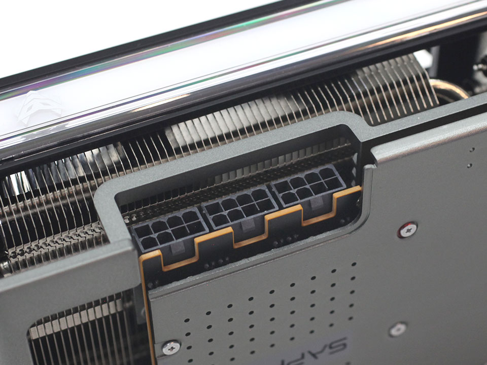
The card uses a classic triple 8-pin power input config, rated for 525 W maximum power. NVIDIA on the other hand uses the new 12+4 pin ATX 12VHPWR connector, which is rated for up to 600 W of power draw.

This dual BIOS switch lets you toggle between the default BIOS and a "secondary" BIOS. Sapphire doesn't give this BIOS any proper name, it runs the card at slightly lower clock speeds, no idea why we need a second BIOS for that. The lower clocks result in a small decrease in temperatures, fan speed and noise levels.
With this generation, Sapphire is including their software BIOS switch feature, too. The BIOS switch has three positions: left-most = default BIOS, middle = secondary BIOS, right = software-controlled. In Sapphire's TRIXX software you can now toggle the BIOS selection, without having to open your case or crawl under your desk.
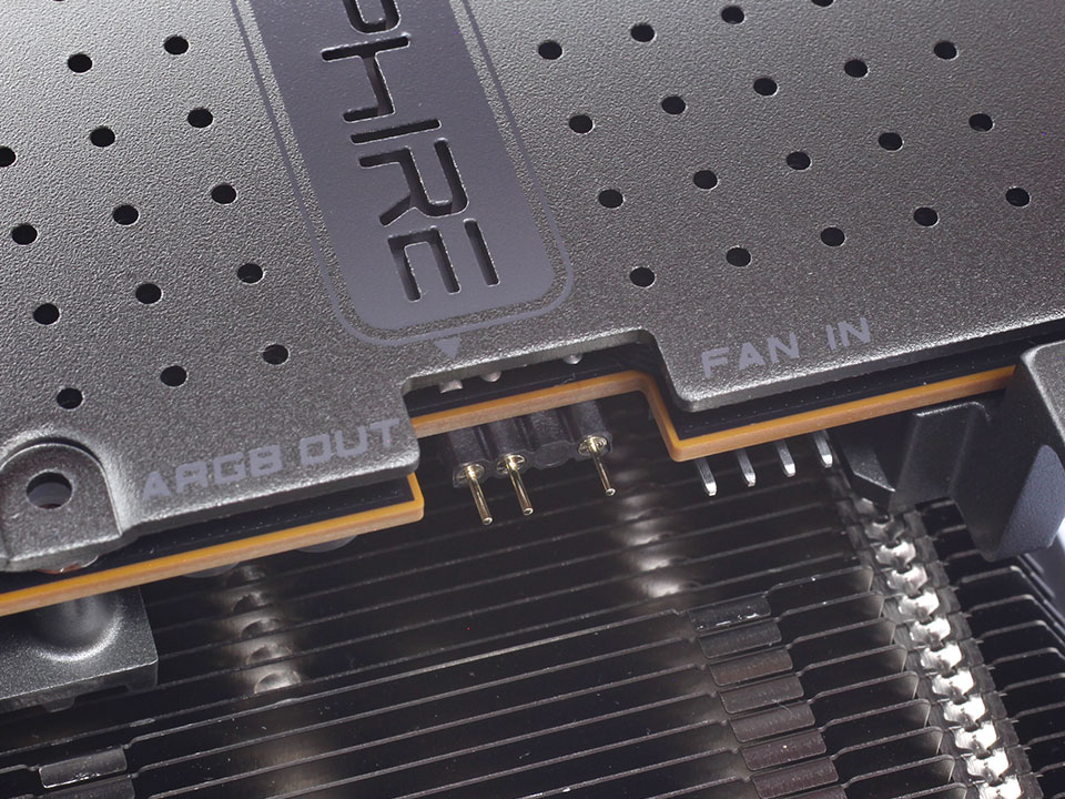
Near the back of the card, Sapphire has placed an ARGB output that lets you sync the rest of the system to the RGB effects of your graphics card. Here you also get a 4-pin header for a case fan that runs synced with the graphics card fan speed. The "Fan In" label is actually a bit misleading, I would have called it "Fan Out," or "External Fan," or similar.
Teardown
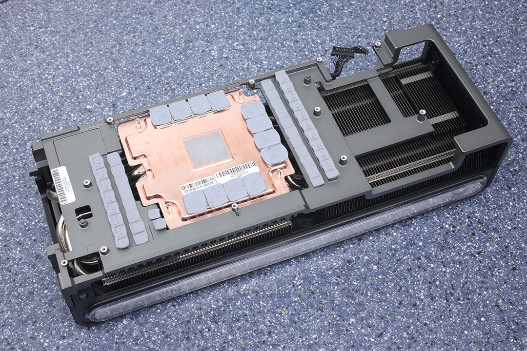

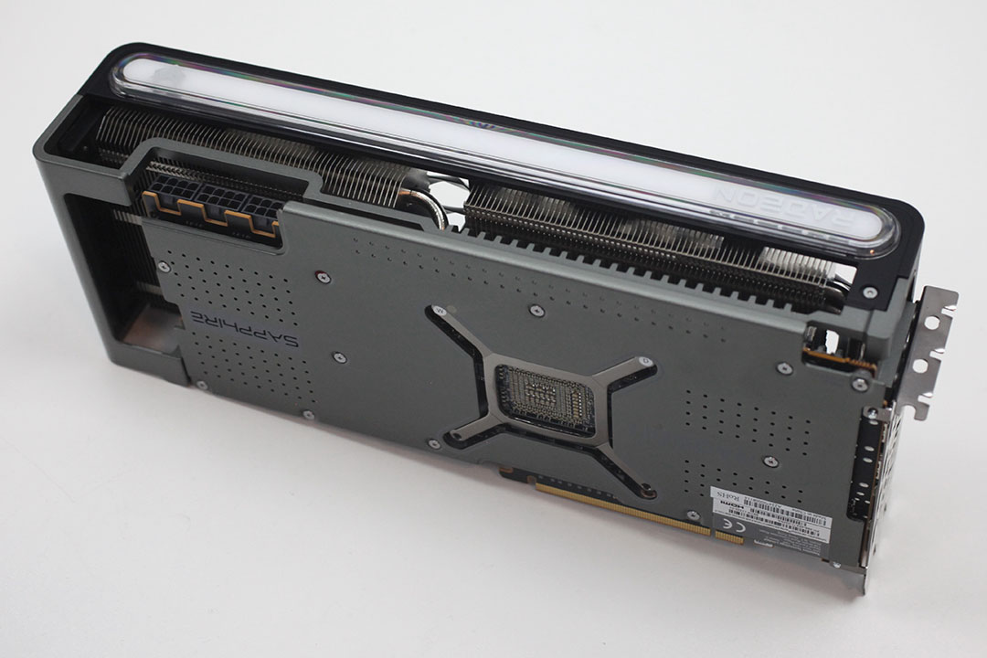
The main heatsink provides cooling for the GPU chip, memory chips and VRM circuitry. Unlike many other cards which use a classic heatsink baseplate, Sapphire has installed a vapor-chamber baseplate, which soaks up the heat and moves it to the heatpipes quickly. Seven heatpipes then transfer heat to the cooling fins.
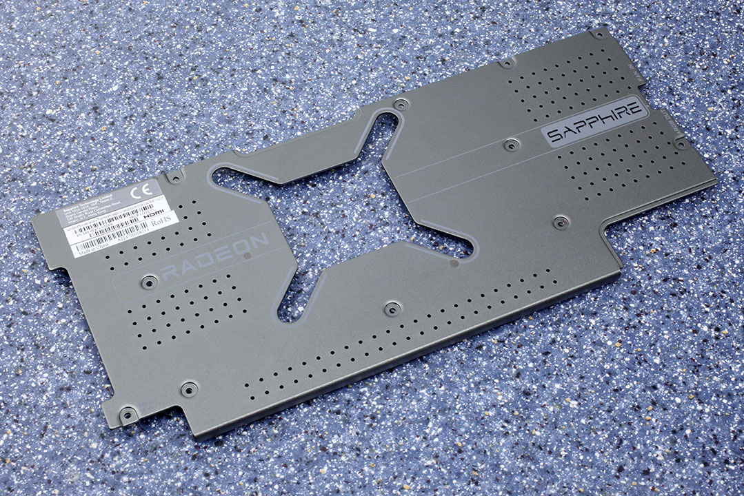
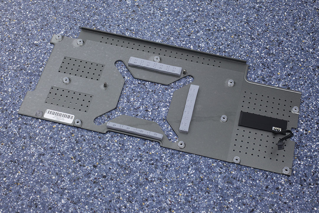
The backplate is made from thick metal and of excellent build quality. It protects the card against damage during installation and handling. Note the thermal pads and the cable for the RGB element.
High-resolution PCB Pictures
These pictures are for the convenience of volt modders and people who would like to see all the finer details on the PCB. Feel free to link back to us and use these in your articles, videos or forum posts.

High-resolution versions are also available (front, back).
Our Patreon Silver Supporters can read articles in single-page format.
May 5th, 2025 07:26 EDT
change timezone
Latest GPU Drivers
New Forum Posts
- Question about photos (3)
- What phone you use as your daily driver? And, a discussion of them. (1662)
- Request for advice [Big Build] (56)
- Windows 12 (167)
- Forza Motorsport discussion thread (228)
- Vertical mice in gaming (15)
- Hundreds of WHEA-17 Hardware Errors per minute? (1)
- Can't find BIOS for RX580 2048SP (8)
- gigabyte rtx 3070 fans are either at 0 rpm or at max rpm (GV-N3070GAMING OC-8GD) (0)
- RX 9000 series GPU Owners Club (643)
Popular Reviews
- ASUS ROG Maximus Z890 Hero Review
- ASUS Radeon RX 9070 XT TUF OC Review
- Clair Obscur: Expedition 33 Performance Benchmark Review - 33 GPUs Tested
- Montech HS02 PRO Review
- NVIDIA GeForce RTX 5060 Ti 8 GB Review - So Many Compromises
- Seasonic Vertex GX 850 W Review
- Upcoming Hardware Launches 2025 (Updated Apr 2025)
- ASUS GeForce RTX 5090 Astral Liquid OC Review - The Most Expensive GPU I've Ever Tested
- Sapphire Radeon RX 9070 XT Nitro+ Review - Beating NVIDIA
- AMD Ryzen 7 9800X3D Review - The Best Gaming Processor
Controversial News Posts
- AMD Radeon RX 9060 XT to Roll Out 8 GB GDDR6 Edition, Despite Rumors (129)
- NVIDIA Sends MSRP Numbers to Partners: GeForce RTX 5060 Ti 8 GB at $379, RTX 5060 Ti 16 GB at $429 (128)
- NVIDIA Launches GeForce RTX 5060 Series, Beginning with RTX 5060 Ti This Week (115)
- Nintendo Confirms That Switch 2 Joy-Cons Will Not Utilize Hall Effect Stick Technology (105)
- NVIDIA PhysX and Flow Made Fully Open-Source (95)
- Sony Increases the PS5 Pricing in EMEA and ANZ by Around 25 Percent (84)
- Parts of NVIDIA GeForce RTX 50 Series GPU PCB Reach Over 100°C: Report (78)
- Intel "Bartlett Lake-S" Gaming CPU is Possible, More Hints Appear for a 12 P-Core SKU (77)