 67
67
WD Black SN850 1 TB SSD Review - The Fastest SSD
(67 Comments) »Introduction
Western Digital (or simply WD) is the world's largest manufacturer of storage solutions, mostly known for their wide range of hard disk offerings. With their acquisition of SanDisk in 2016, WD became one of the largest manufacturers for flash storage, too.

Today, we're reviewing the WD Black SN850 SSD, which is a high-end M.2 NVMe drive that introduces support for the PCI-Express 4.0 interface. Internally, the WD Black SN850 uses the new eight-channel SanDisk 20-82-10035-A1 controller, which Western Digital refers to as the WD G2. The flash chips are made by Toshiba and 96-layer TLC. A Nanya DRAM chip provides 1 GB of storage for the mapping tables of the SSD.
The WD Black SN850 comes in capacities of 500 GB ($120), 1 TB ($230), and 2 TB ($450). Endurance for these models is set to 300 TBW, 600 TBW, and 1200 TBW respectively. WD also offers a separate SKU that comes with a preinstalled heatsink, for a small price increase, of course. WD provides a five-year warranty for the SN850.
| Specifications: WD Black SN850 1 TB SSD | |
|---|---|
| Brand: | WD / Western Digital |
| Model: | WDS100T1X0E-00AFY0 |
| Capacity: | 1000 GB (931 GB usable) 24 GB additional overprovisioning |
| Controller: | SanDisk 20-82-10035-A1 / WD G2 |
| Flash: | Toshiba 96-layer 3D TLC BiCS4 Rebranded as SanDisk |
| DRAM: | 1x 1 GB Nanya DDR4-2666 NT5AD512M16C4-HR |
| Endurance: | 600 TBW |
| Form Factor: | M.2 2280 |
| Interface: | PCIe Gen 4 x4, NVMe 1.4 |
| Device ID: | WDS100T1X0E-00AFY0 |
| Firmware: | 611110WD |
| Warranty: | Five years |
| Price at Time of Review: | $230 / 23 cents per GB |
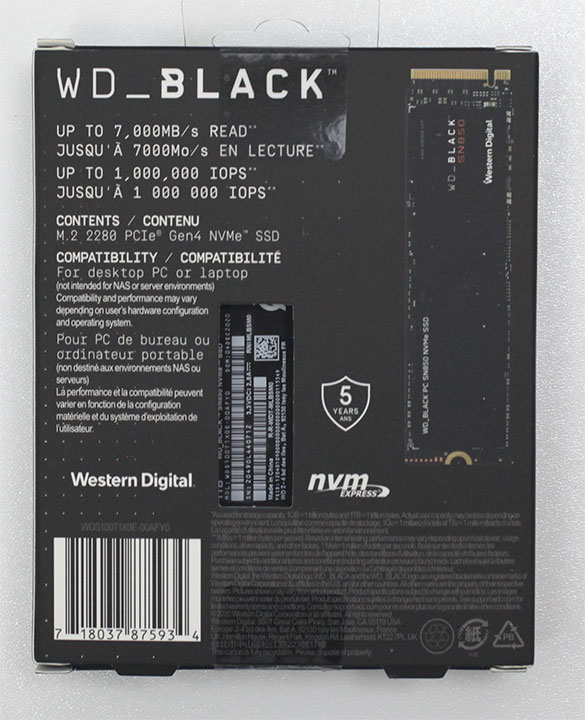
Packaging

The Drive
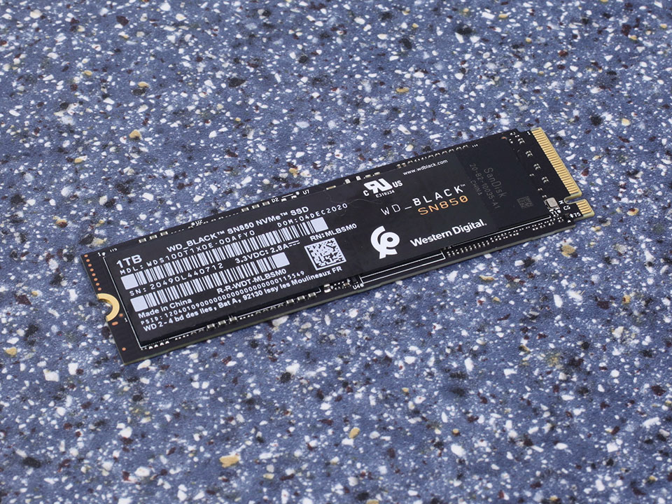

The drive uses the M.2 2280 form factor, which makes it 22 mm wide and 80 mm long.

While most other M.2 NVMe SSDs transfer data over the PCI-Express 3.0 x4 interface, the WD Black SN850 connects to the host system over a PCI-Express 4.0 x4 interface, which doubles the theoretical bandwidth.

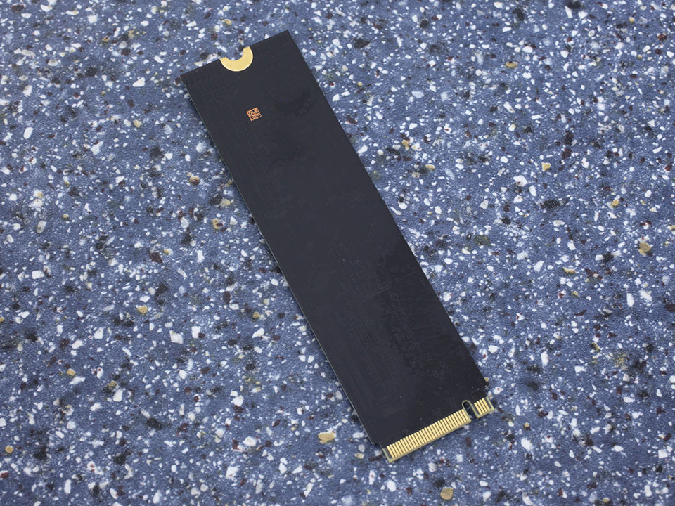
On the PCB, you'll find the controller, two flash chips, and one DRAM chip; the other side of the PCB is empty.
Chip Component Analysis
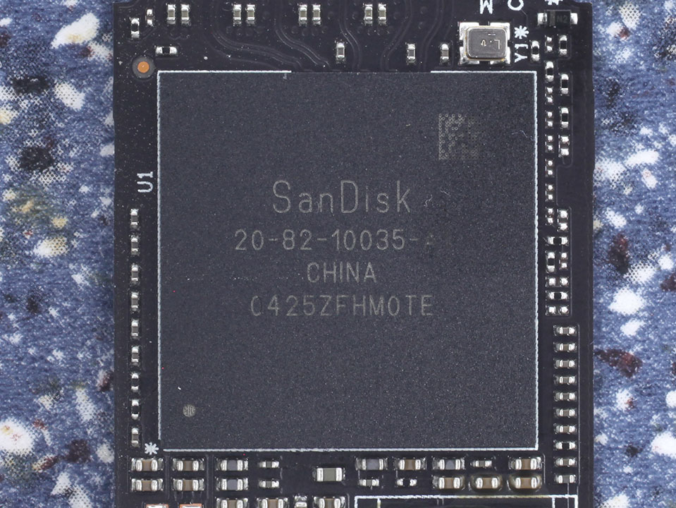
This is SanDisk's new PCIe Gen 4 controller. WD gave it the marketing name "WD G2." The controller uses eight flash channels and has support for NVMe 1.4, TLC, and DDR4 DRAM.
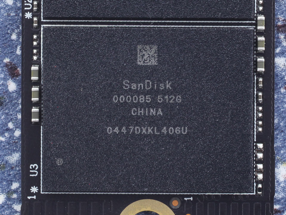
The two flash chips are Toshiba 96-layer 3D TLC NAND. Each chip has a capacity of 512 GB.

A Nanya DDR4-2666 chip provides 1 GB of fast DRAM storage for the controller to store the mapping tables.
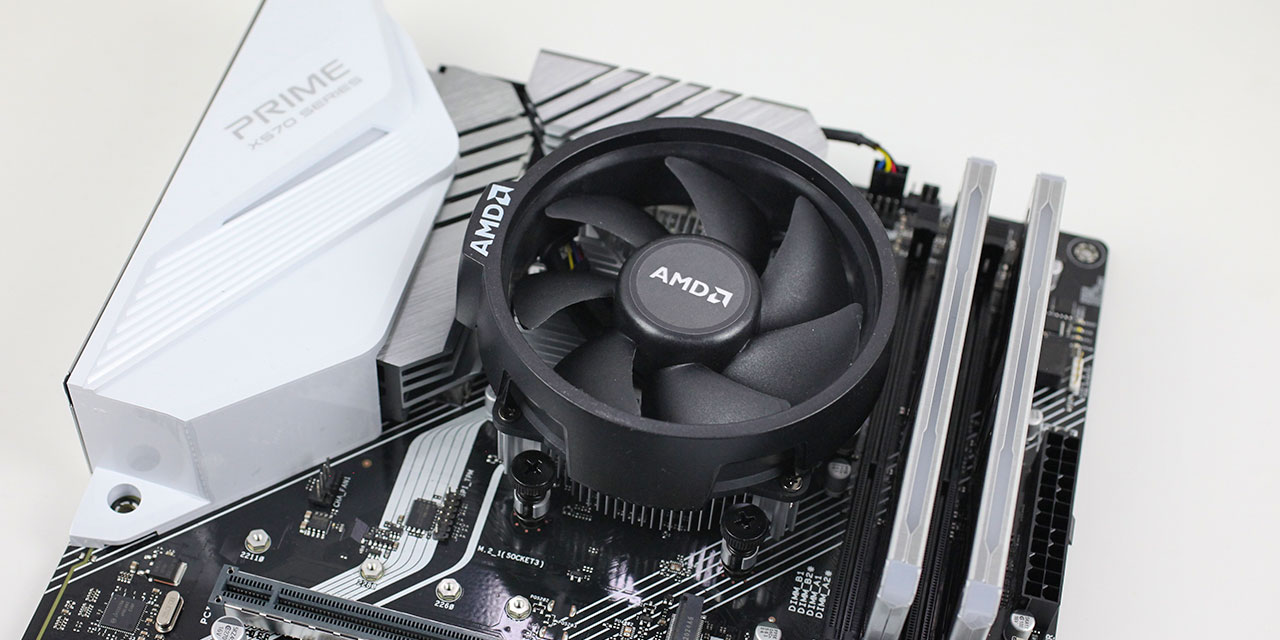
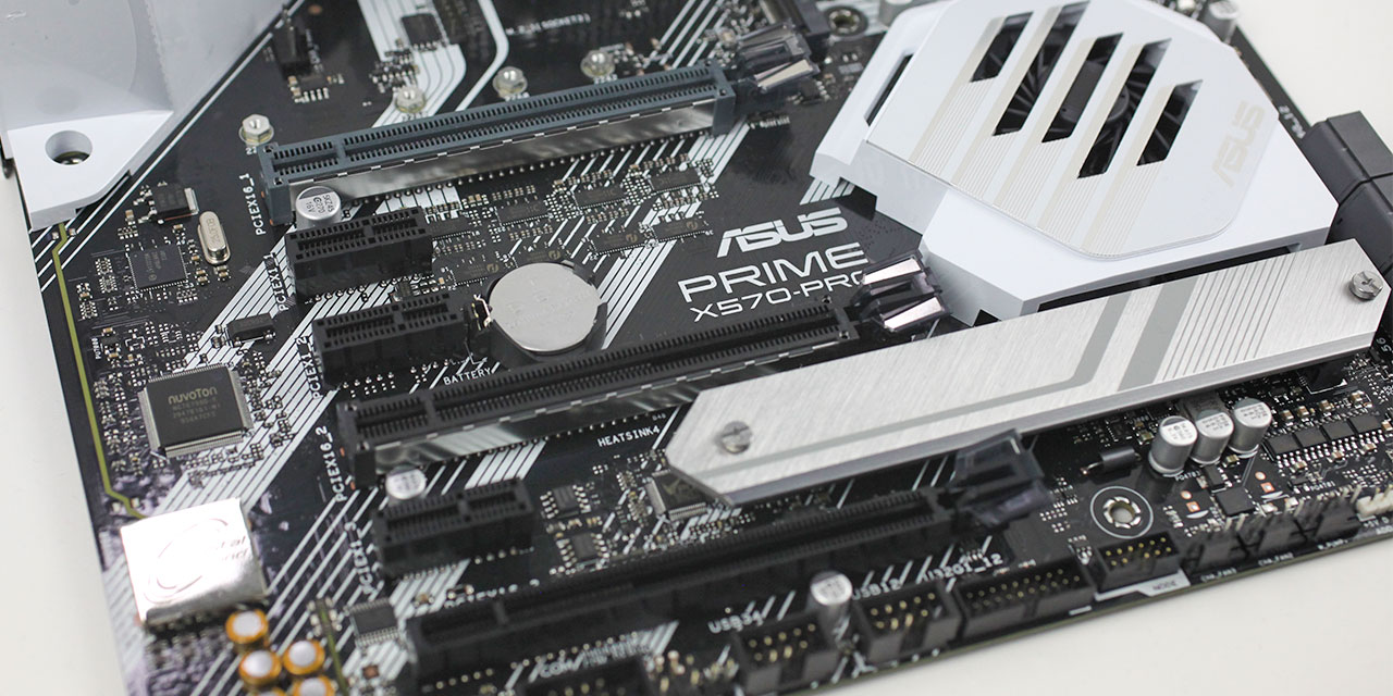
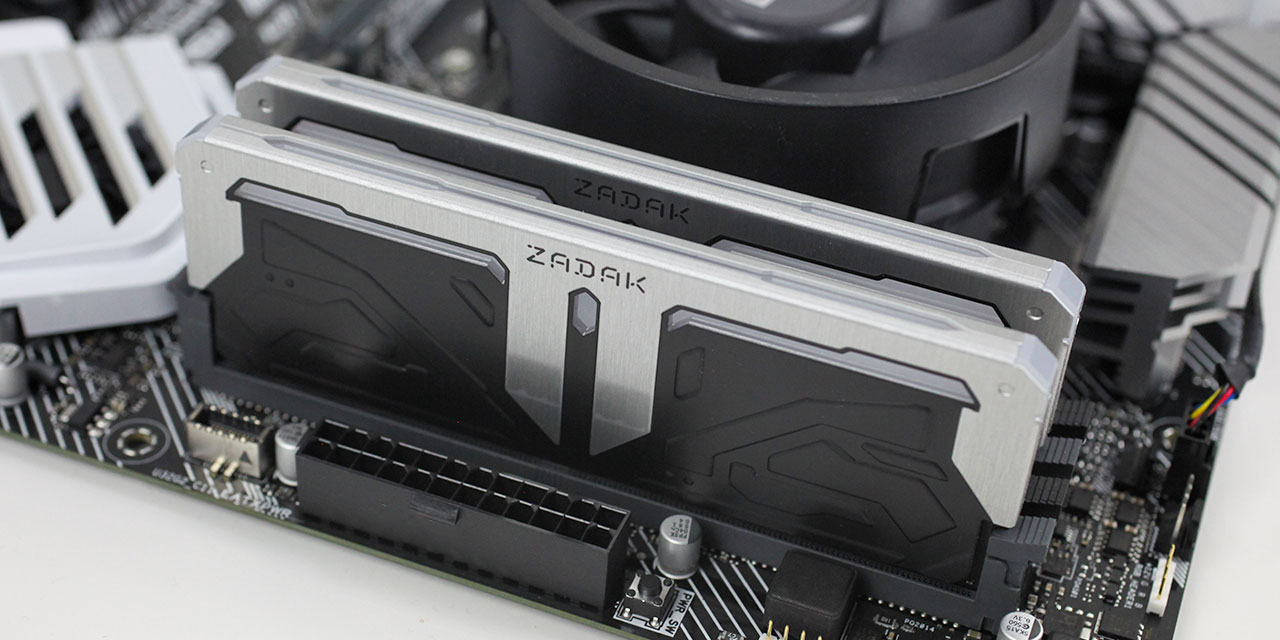
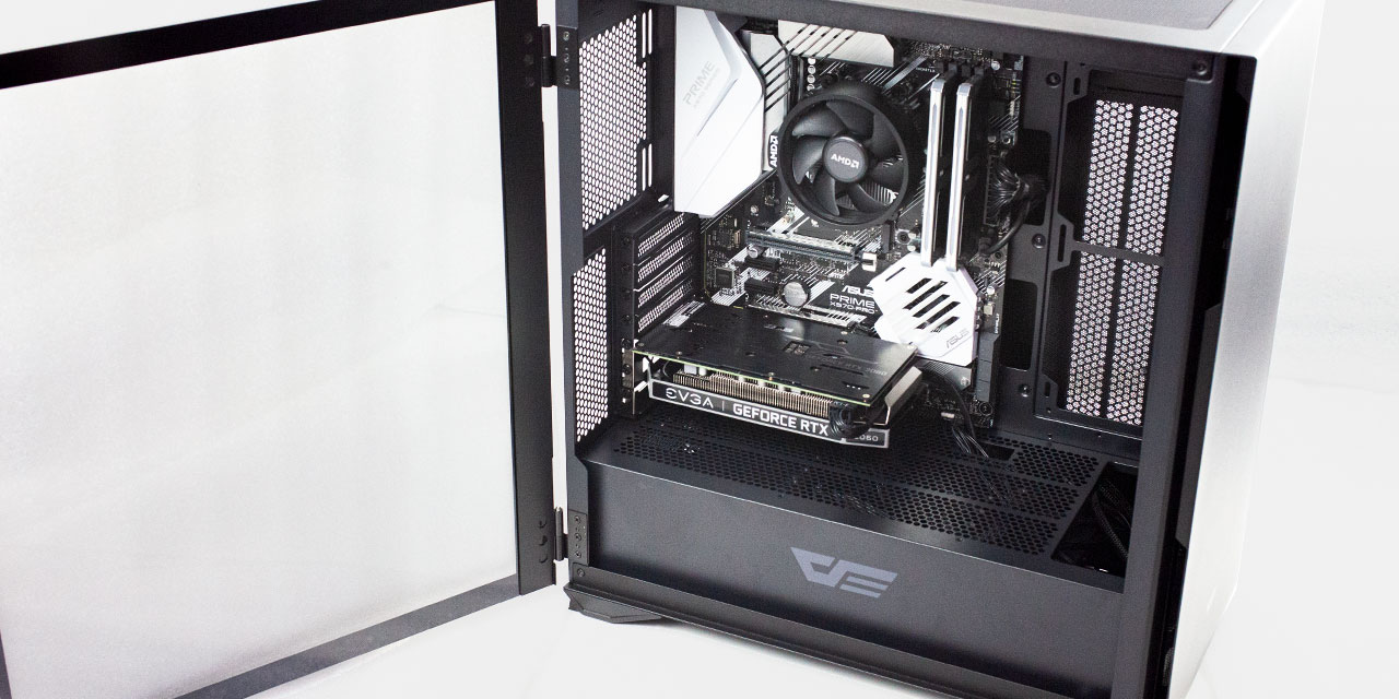
Test Setup
| Test System SSD 2021 | |
|---|---|
| Processor: | AMD Ryzen 3 3300X @ 4.3 GHz Zen 2, 16 MB Cache |
| Motherboard: | ASUS Prime X570-Pro BIOS 2606 / AGESA 1.0.8.0 |
| Memory: | Zadak Spark RGB, 16 GB DDR4 @ 3200 MHz 16-18-18-38 |
| Graphics: | EVGA GeForce RTX 2060 KO 6 GB |
| Case: | DarkFlash DLX22 |
| Operating System: | Windows 10 Professional 64-bit Version 2004 (May 2020 Update) |
| Drivers: | AMD Chipset: 2.07.14.327 NVIDIA: 452.06 WHQL |
Our Patreon Silver Supporters can read articles in single-page format.
May 5th, 2025 09:11 EDT
change timezone
Latest GPU Drivers
New Forum Posts
- It's happening again, melting 12v high pwr connectors (1058)
- Windows 11 General Discussion (6024)
- Is RX 9070 VRAM temperature regular value or hotspot? (375)
- Are the 8 GB cards worth it? (866)
- Can't connecte my xbox controller to my pc (ugreen bt adapter) (4)
- Microcenter GPU Stock status (101)
- Windows 12 (173)
- Low budget psu for medium high loads (under 400 watt usage) (24)
- [AV1, AV2, AV3 codecs...] Have they given up on the AOMedia project? (20)
- What are you playing? (23546)
Popular Reviews
- ASUS ROG Maximus Z890 Hero Review
- ASUS Radeon RX 9070 XT TUF OC Review
- Clair Obscur: Expedition 33 Performance Benchmark Review - 33 GPUs Tested
- Montech HS02 PRO Review
- NVIDIA GeForce RTX 5060 Ti 8 GB Review - So Many Compromises
- Seasonic Vertex GX 850 W Review
- Upcoming Hardware Launches 2025 (Updated Apr 2025)
- ASUS GeForce RTX 5090 Astral Liquid OC Review - The Most Expensive GPU I've Ever Tested
- Sapphire Radeon RX 9070 XT Nitro+ Review - Beating NVIDIA
- AMD Ryzen 7 9800X3D Review - The Best Gaming Processor
Controversial News Posts
- AMD Radeon RX 9060 XT to Roll Out 8 GB GDDR6 Edition, Despite Rumors (131)
- NVIDIA Sends MSRP Numbers to Partners: GeForce RTX 5060 Ti 8 GB at $379, RTX 5060 Ti 16 GB at $429 (128)
- NVIDIA Launches GeForce RTX 5060 Series, Beginning with RTX 5060 Ti This Week (115)
- Nintendo Confirms That Switch 2 Joy-Cons Will Not Utilize Hall Effect Stick Technology (105)
- NVIDIA PhysX and Flow Made Fully Open-Source (95)
- Sony Increases the PS5 Pricing in EMEA and ANZ by Around 25 Percent (84)
- Parts of NVIDIA GeForce RTX 50 Series GPU PCB Reach Over 100°C: Report (78)
- Intel "Bartlett Lake-S" Gaming CPU is Possible, More Hints Appear for a 12 P-Core SKU (77)