Friday, August 14th 2020

NVIDIA GeForce RTX 3090 "Ampere" Alleged PCB Picture Surfaces
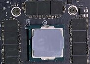
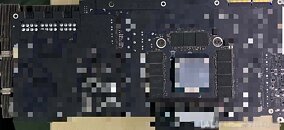
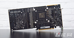
As we are getting close to September 1st, the day NVIDIA launches its upcoming GeForce RTX graphics cards based on Ampere architecture, we are getting even more leaks. Today, an alleged PCB of the NVIDIA's upcoming GeForce RTX 3090 has been pictured and posted on social media. The PCB appears to be a 3rd party design coming from one of NVIDIA's add-in board (AIB) partners - Colorful. The picture is blurred out on the most of the PCB and has Intel CPU covering the GPU die area to hide the information. There are 11 GDDR6X memory modules covering the surrounding of the GPU and being very near it. Another notable difference is the NVLink finger change, as there seems to be the new design present. Check out the screenshot of the Reddit thread and PCB pictures below:More pictures follow:
Source:
VideoCardz


72 Comments on NVIDIA GeForce RTX 3090 "Ampere" Alleged PCB Picture Surfaces
edit: okay reading first, that IS an intel CPU. wtf is the point of the pictures then?
Were there also no credible leaks until the very reveal date?
Quite an electric heater
Here is a better image. Maybe hiding more Ram?
ooops....deleted
Not long now either way, looks like the performance goal posts are about to move again.
media-www.micron.com/-/media/client/global/documents/products/technical-marketing-brief/ultra_bandwidth_solutions_tech_brief.pdf?rev=16ecd1bb494f4a958810146858c02bab
This lends credibility to this PCB, it shows 24 memory dies, 12 on each side, which lines up with the Micron document
It's a newer 10th gen i3 Intel CPU.... probably using MS Paint....
Clearly the IHS is identical and even the markings on the side of the chip are identical...why would Nvidia put guide slots on the side of their new GPU when it doesn't have an INTEL socket... plus you can even see the markings of the IHS on the side where it was already mounted....lame
Edit: GDDR6X (PAM4) trades trace SNR for bandwidth, hence back drill VIAs & novel RAM module layout.