Monday, January 4th 2021

AMD Patents Chiplet Architecture for Radeon GPUs

On December 31st, AMD's Radeon group has filed a patent for a chiplet architecture of the GPU, showing its vision about the future of Radeon GPUs. Currently, all of the GPUs available on the market utilize the monolithic approach, meaning that the graphics processing units are located on a single die. However, the current approach has its limitations. As the dies get bigger for high-performance GPU configurations, they are more expensive to manufacture and can not scale that well. Especially with modern semiconductor nodes, the costs of dies are rising. For example, it would be more economically viable to have two dies that are 100 mm² in size each than to have one at 200 mm². AMD realized that as well and has thus worked on a chiplet approach to the design.

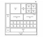
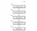
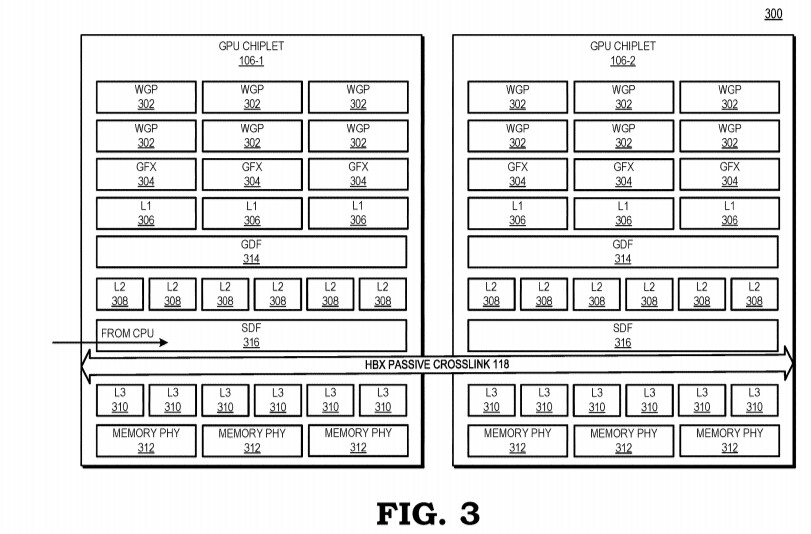
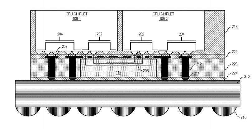
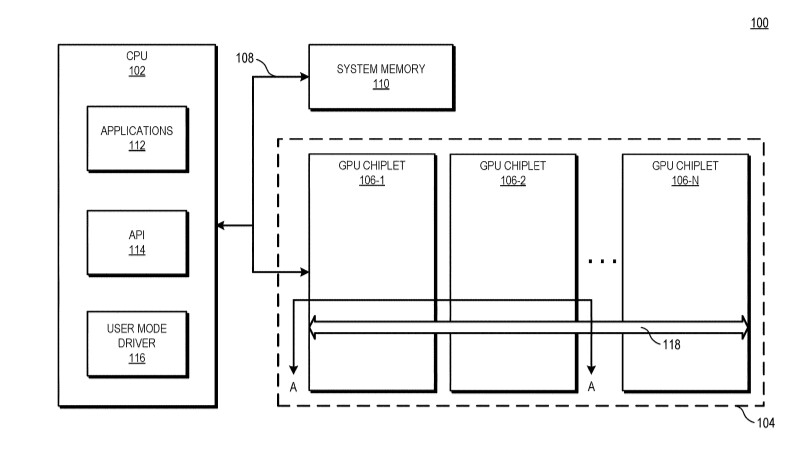
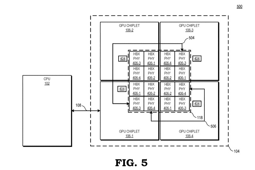
AMD reports that the use of multiple GPU configuration is inefficient due to limited software support, so that is the reason why GPUs were kept monolithic for years. However, it seems like the company has found a way to go past the limitations and implement a sufficient solution. AMD believes that by using its new high bandwidth passive crosslinks, it can achieve ideal chiplet-to-chiplet communication, where each GPU in the chiplet array would be coupled to the first GPU in the array. All the communication would go through an active interposer which would contain many layers of wires that are high bandwidth passive crosslinks. The company envisions that the first GPU in the array would communicably be coupled to the CPU, meaning that it will have to use the CPU possibly as a communication bridge for the GPU arrays. Such a thing would have big latency hit so it is questionable what it means really.
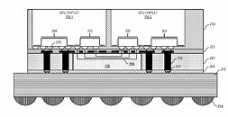
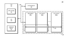
The patent also suggests that each GPU chiplet uses its own Last Level Cache (LLC), instead of separate LLCs for each GPU, so each of the LLCs is communicably coupled and the cache remains coherent across all chiplets. Rumors suggest that we are going to see the first chiplet-based architecture from AMD as successor to the RDNA3 generation, so it will happen in the coming years. AMD already has experience with chiplets from its processors, with Ryzen processors being the prime example. We just need to wait and see how it will look once it arrives for GPUs.
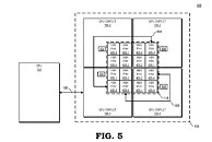
Sources: Free Patents Online, via VideoCardz
Add your own comment

69 Comments on AMD Patents Chiplet Architecture for Radeon GPUs

#1
Verpal
Predictable.

But, When?
Posted on Reply
#2
laszlo
a move before NV ? just to make them pay if they'll go same path?
Posted on Reply
#3
FinneousPJ
VerpalPredictable.

But, When?
I predict 2022 :)
Posted on Reply
#4
londiste
Pretty sure this will be used for compute designs first, for at least a generation or two before we see this in consumer GPU.
They also need something clever to avoid the latency hits, the memory duplication issues etc.
Posted on Reply
#5
Vya Domus
londistePretty sure this will be used for compute designs first, for at least a generation or two before we see this in consumer GPU.
They also need something clever to avoid the latency hits, the memory duplication issues etc.
I don't see why memory duplication would be an issue, CUs will still be accessing global memory in the same way as before. Neither will be latency, CUs don't need to communicate among each other.
Posted on Reply
#7
dj-electric
That chip to chip interconnect better be the speed of light.
Posted on Reply
#8
Vya Domus
dj-electricThat chip to chip interconnect better be the speed of light.
Like I said above, it doesn't need to, in fact you need very little chiplet to chiplet communication as CUs don't need to communicate.

GPUs aren't CPUs where core to core communication happens all the time.
Posted on Reply
#9
londiste
Vya DomusI don't see why memory duplication would be an issue, CUs will still be accessing global memory in the same way as before. Neither will be latency, CUs don't need to communicate among each other.
But memory is not global, each chiplet has its own memory controller.
CUs might not need to communicate more than they do right now but chiplets definitely need to, which is the point of the patent.

But if that is the case, what is the point of this patent? Using a faster interconnect? I do not recall if AMD has released something with fast interconnect but Nvidia's attempts with NVLink are not too encouraging, effectively leaving leading to the same issues as Crossfire/SLI always had.
Posted on Reply
#10
Vya Domus
londisteBut memory is not global, each chiplet has its own memory controller.
CUs might not need to communicate more than they do right now but chiplets definitely need to, which is the point of the patent.
What do you mean it's not global ? You do know monolithic GPUs already have multiple memory controllers that serve different CUs, right ? If you divide the chip nothing changes, you still have multiple controllers to feed multiple CUs in each chiplet.

Point of the patent ? I don't know, go ask their lawyers. Apple patented a rectangle with rounded edges so I don't think there is much point in wondering why something gets patented.
Posted on Reply
#11
Kohl Baas
I wonder what people think who woted "against" the chiplet design. What do they think the future will/should be with a realistic point of view. I mean manufacturing costs grow almost exponentially, so yielads are key. You have to go smaller anyway or else the prices will go to unbearable heights. And there is a limit how much more power you can squeeze out generation to generation while maintaining or even shrinking the size of the DIE. The MCM is the best solution to make the DIE small for the highest possible yields but keep the GPU big by stacking/combining multiple DIEs.
Posted on Reply
#12
evernessince
londistePretty sure this will be used for compute designs first, for at least a generation or two before we see this in consumer GPU.
They also need something clever to avoid the latency hits, the memory duplication issues etc.
AMD already employs advanced cache coherency with RDNA2. CUs not only have access to the infinity cache and their local L1 and L2 caches, but also any neighboring L1 / L2 caches as well. RDNA2 also stores data intelligently using this as well. For example, it will store data that's frequently used together in a set of CUs that are close to each other. Not only does this increase effective cache size by removing duplicates, it also increases effective bandwidth. Just another trick AMD used to compensate for the slower memory it used.

I would not be surprised if AMD's chiplet based GPUs also had cache coherency between the dies. Being able to ensure that data is in the caches closest to where it's needed across multiple dies is huge for a chiplet architecture. On top of that you also avoid duplicates in L1 / L2 caches across dies and CU groups.
Kohl BaasI wonder what people think who woted "against" the chiplet design. What do they think the future will/should be with a realistic point of view. I mean manufacturing costs grow almost exponentially, so yielads are key. You have to go smaller anyway or else the prices will go to unbearable heights. And there is a limit how much more power you can squeeze out generation to generation while maintaining or even shrinking the size of the DIE. The MCM is the best solution to make the DIE small for the highest possible yields but keep the GPU big by stacking/combining multiple DIEs.
Not sure on stacking (as in vertically) in regards to high power dies. If the surface area of a vertically stacked die is smaller than a monolithic one, you are looking at more heat in a smaller area. The bottom die is basically insulated under the top die and does not get direct contact either. I feel like you need to make some serious design considerations for vertical stacking, much more so than AMD's chiplet based approach.
Posted on Reply
#13
yeeeeman
Nice. nvidia and Intel already have this in labs. So why is this is a news when amd does it and when others do it it is not?
Posted on Reply
#14
DeathtoGnomes
yeeeemanNice. nvidia and Intel already have this in labs. So why is this is a news when amd does it and when others do it it is not?
what are you saying here? nvidia and intel has news stories written about this but amd doesnt?

--
Posted on Reply
#15
londiste
DeathtoGnomeswhat are you saying here? nvidia and intel has news stories written about this but amd doesnt?
These stories come and go.
One of the last/bigger Nvidia papers on MCM GPU is from a couple years ago - research.nvidia.com/sites/default/files/publications/ISCA_2017_MCMGPU.pdf. The current rumor is that Hopper will be MCM.
Intel showed/leaked the MCM Xe HP pictures earlier this year.
AMD has been talking about MCM on and off since... R600 back in 2007? There is always hope that this gets a good working implementation.

Intel is going for MCM in HPC segment. Nvidia's Hopper details are scarce but entirely possible that it will be a compute-focused things (like Volta). AMD is the odd one out that doesn't have any specific enough rumors.

What has changed now is interconnects and more recently - packaging technologies. NVLink and IF have existed for a while. Now 2.5D packaging and things like EMIB are becoming "mainstream" enough to use. All that helps immensely with setting up the required communication.
Posted on Reply
#16
DeathtoGnomes
londisteAMD has been talking about MCM on and off since... R600 back in 2007? There is always hope that this gets a good working implementation.
its been longer than that, hasnt it? Since before the X2 dual GPU concepts. MCM implementation has always needed other tech to catch up to make it "better" than current designs, in AMDs view, software has held them back.
Posted on Reply
#17
londiste
DeathtoGnomesits been longer than that, hasnt it? Since before the X2 dual GPU concepts. MCM implementation has always needed other tech to catch up to make it "better" than current designs, in AMDs view, software has held them back.
It has been longer. 3dfx's SLI, some (rare) dual-GPU Voodoo2 cards and their planned multi-GPU Voodoo4/5 cards were a thing since 1998 or so. With the changes in GPUs and rendering methods that naive of an implementation no longer worked. The holy grail for gaming is still an MCM GPU that would appears as single GPU to software or API.

MCM was specifically stated as a possible goal with R600 and small chips strategy. It didn't pan out too well (for any manufacturer so far).
Posted on Reply
#18
Verpal
londisteIt has been longer. 3dfx's SLI, some (rare) dual-GPU Voodoo2 cards and their planned multi-GPU Voodoo4/5 cards were a thing since 1998 or so. With the changes in GPUs and rendering methods that naive of an implementation no longer worked. The holy grail for gaming is still an MCM GPU that would appears as single GPU to software or API.

MCM was specifically stated as a possible goal with R600 and small chips strategy. It didn't pan out too well (for any manufacturer so far).
Kinda sad NVIDIA killed off their internal 3DFX guys, SLI is over.
Posted on Reply
#19
medi01
VerpalPredictable.

But, When?
1.5 years ago.
Notably, before they've acquired Xilinx.
Vya DomusLike I said above, it doesn't need to, in fact you need very little chiplet to chiplet communication as CUs don't need to communicate.
You are essentially saying "we could have had chiplet based GPUs for ages", which... is not really true, I thought.

Perhaps things have changed with that "infinity cache" bit.

Thrilling if true.

Posted on Reply
#20
Vya Domus
medi01You are essentially saying "we could have had chiplet based GPUs for ages", which... is not really true, I thought.
There just wasn't a need for them. The only proper use of chiplets is when you've exhausted every other trick in the book and you simply can't make a faster chip without colossal costs, that's why AMD debuted chiplets in CPUs with their server products first because it was the only way to beat Intel in a cost effective fashion.
Posted on Reply
#21
Valantar
The company envisions that the first GPU in the array would communicably be coupled to the CPU, meaning that it will have to use the CPU possibly as a communication bridge for the GPU arrays. Such a thing would have big latency hit so it is questionable what it means really.
I think this is entirely misunderstood. This likely means that the PCIe link between CPU and GPU is only between the CPU and the first/primary GPU chiplet (rather than to all chiplets simultaneously). Which makes complete sense, obviously.
Posted on Reply
#22
Vya Domus
ValantarThis likely means that the PCIe link between CPU and GPU is only between the CPU and the first/primary GPU chiplet (rather than to all chiplets simultaneously). Which makes complete sense, obviously.
Or maybe not. "Primary chiplet" implies that there is a scheduler in it which either doesn't exist or is not enabled in the other one but that's a really strange asymmetric way to do it and it also involves a lot of chiplet-to-chiplet communication. It is totally within reason that both chiplets have their own scheduler and they both receive instructions/data off the PCIe bus.
Posted on Reply
#23
Valantar
Vya DomusOr maybe not. "Primary chiplet" implies that there is a scheduler in it which either doesn't exist or is not enabled in the other one but that's a really strange asymmetric way to do it. It is totally within reason that both chiplets have their own scheduler and they both receive instructions/data off the PCIe bus.
The first sentence of the linked patent is literally this:
1. A system, comprising: a central processing unit (CPU) communicably coupled to a first graphics processing unit (GPU) chiplet of a GPU chiplet array, wherein the GPU chiplet array includes: the first GPU chiplet communicably coupled to the CPU via a bus; and a second GPU chiplet communicably coupled to the first GPU chiplet via a passive crosslink, wherein the passive crosslink is dedicated for inter-chiplet communications.
In other words, a system consisting of a CPU with a PCIe link to a primary GPU chiplet, which itself has a passive crosslink connecting it to the other chiplet(s). There is zero mention of any connection between the CPU and chiplets beyond the first.
Posted on Reply
#24
Vya Domus
ValantarIn other words, a system consisting of a CPU with a PCIe link to a primary GPU chiplet, which itself has a passive crosslink connecting it to the other chiplet(s). There is zero mention of any connection between the CPU and chiplets beyond the first.
It does look like that's the case but it's still strange that they chose to do it this way. This means the chiplet connected to the bus has to do a lot of extra scheduling and since I imagine they'd all have to be identical this seems rather wasteful and could generate a lot of overheard.
Posted on Reply
#25
londiste
Vya DomusIt does look like that's the case but it's still strange that they chose to do it this way. This means the chiplet connected to the bus has to do a lot of extra scheduling and since I imagine they'd all have to be identical this seems rather wasteful and could generate a lot of overheard.
Why does the first chiplet need to do scheduling? First die can do communication and maybe some basic scheduling, leaving rest to schedulers on the chiplets. Didn't GPU in Xbox One have multiple GCPs?
Posted on Reply
Add your own comment
May 21st, 2024 19:24 EDT change timezone

New Forum Posts

Popular Reviews

Controversial News Posts