Friday, June 11th 2021

AMD Shares New Details on Their 3D V-Cache Tech for Zen 3+

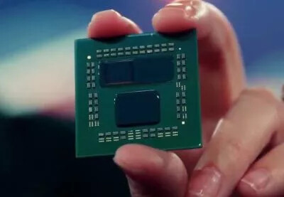
AMD via its official YouTube has shared a video that goes into slightly more detail on their usage of V-Cache on the upcoming Zen 3+ CPUs. Firstly demoed to the public on AMD's Computex 2021 event, the 3D V-Cache leverages TSMC's SoIC stacking technology, which enables silicon developments along the Z axis, instead of the more usual footprint increase along the X axis. The added 3D V-Cache, which was shown in Computex as being deployed in a prototype Ryzen 9 5900X 12-core CPU, adds 64 MB of L3 cache to each CCX (the up-to-eight-cores core complex on AMD's latest Zen design), basically tripling the amount of L3 cache available for the CPU. This, in turn, was shown to increase FPS in games quite substantially (somewhere around 15%), as games in particular are sensitive to this type of CPU resources.

The added information explains that there is no usage of microbumps - instead, there is a perfect alignment between the bottom layer (with the CCX) and the top layer (the L3 cache) which enables the bonding process to occur naturally via the TSVs (Through Silicon Vias) already present in the silicon, in a zero-gap manner, between both halves of the CPU-cache sandwich. To enable this, AMD flipped the CCX upside down (the core complex now faces the bottom of the chip, instead of the top), shaved 95% of the silicon on top of the upside-down core complexes, and then attaches the 3D V-Cache chips on top of this formation. This also has the added bonus of decreasing the distance between the L3 cache and the CCX (the distance between both in the Z axis is around 1,000 times smaller than if the L3 cache was deployed in the classical X axis), which decreases power consumption, temperatures, and latency, allowing for further increases to system performance. Look after the break for the full video.
Source: AMD
Add your own comment

37 Comments on AMD Shares New Details on Their 3D V-Cache Tech for Zen 3+

#1
TumbleGeorge
AMD have quite strong cards hidden in the sleeve .... From time to time, they take out some and make Intel look pathetic.
Posted on Reply
#2
stimpy88
Not bad AMD! an up to 15% performance increase is more than intel does in 3 generations of CPUs, and this is only with cache, not IPC! Combine both in Zen4, and I see more fun ahead for Intel.

I REALLY hope that Zen3+ is for AM4, as I don't like what I'm seeing with DDR5. I think it's just too early for AMD to abandon AM4 and DDR4, at least for this year.
Posted on Reply
#3
mtcn77
I haven't kept the old trolling material, however AMD wasn't the only company targetting 3D stacking, it sure is the first without the shadow of a doubt!
This is the definition of success however way anybody puts it!
Posted on Reply
#4
HTC
stimpy88Not bad AMD! an up to 15% performance increase is more than intel does in 3 generations of CPUs, and this is only with cache, not IPC! Combine both in Zen4, and I see more fun ahead for Intel.

I REALLY hope that Zen3+ is for AM4, as I don't like what I'm seeing with DDR5. I think it's just too early for AMD to abandon AM4 and DDR4, at least for this year.
Something's bothering me: why did AMD use the prototype @ a fixed 4 GHz VS a regular 5900X also @ a fixed 4GHz, instead of the prototype @ "it's normal speed" VS the 5900X @ it's normal speed?

Either they don't yet know what "it's normal speed" will end up being, which is actually quite likely, or this prototype will end up having a lower frequency than the 5900X due to it's new "3D nature", meaning that 15% improvement might not actually be as much as it seems to be.

Ofc, that 15% @ 4 GHz is only with the 3D V-cache without anything else, so it's still possible that the new Zen 3+ CPU could still end up being 15%+ faster than the 5900X WHILE having ... say ... 400 to 500 MHz LESS frequency, depending on WHAT ELSE is being changed VS Zen 3.
Posted on Reply
#5
Tomgang
Yeah i do hope this will be for AM4. This will give me a upgrade choise longer down the road. Now i am on Zen 3.
Posted on Reply
#6
Wirko
Why is everybody assuming that 3D V-Cache is the same as Zen 3+? They could as well be two distinct things.

Like, Zen 3+ being intended for APUs, with several improvements over Zen 3, similar to what Lucienne is for Zen 2. And 3D V-cache for high end Ryzen CPUs, those that can bear the high cost of advanced packaging and additional silicon.
Posted on Reply
#7
Dredi
stimpy88Not bad AMD! an up to 15% performance increase is more than intel does in 3 generations of CPUs, and this is only with cache, not IPC! Combine both in Zen4, and I see more fun ahead for Intel.

I REALLY hope that Zen3+ is for AM4, as I don't like what I'm seeing with DDR5. I think it's just too early for AMD to abandon AM4 and DDR4, at least for this year.
Cache is there just to improve IPC in certain applications. If it didn’t improve IPC, it would be unnecessary.
Posted on Reply
#8
mtcn77
DrediCache is there just to improve IPC in certain applications. If it didn’t improve IPC, it would be unnecessary.
Listen to this gentlement, 10/10 remark...
Cache admittedly improves single threading since it acts like a huge page file.
Posted on Reply
#9
Dredi
mtcn77Listen to this gentlement, 10/10 remark...
Cache admittedly improves single threading since it acts like a huge page file.
Cache also improves IPC in multi threaded applications.
Posted on Reply
#10
TheoneandonlyMrK
HTCSomething's bothering me: why did AMD use the prototype @ a fixed 4 GHz VS a regular 5900X also @ a fixed 4GHz, instead of the prototype @ "it's normal speed" VS the 5900X @ it's normal speed?

Either they don't yet know what "it's normal speed" will end up being, which is actually quite likely, or this prototype will end up having a lower frequency than the 5900X due to it's new "3D nature", meaning that 15% improvement might not actually be as much as it seems to be.

Ofc, that 15% @ 4 GHz is only with the 3D V-cache without anything else, so it's still possible that the new Zen 3+ CPU could still end up being 15%+ faster than the 5900X WHILE having ... say ... 400 to 500 MHz LESS frequency, depending on WHAT ELSE is being changed VS Zen 3.
Orr, AMD yet again are holding something back for a later announcement/sales push.

Plus she could only show a prototype, you realise this isn't even a qualification sample.

It's clearly early in the production cycle ,only an idiot would show all their competitors they're full hand with enough time to do something about it that's competitive?!.


No glue, either , make's me wonder how strong that atomic flatness bonding is, Many of us have used standard set guages , sets of metal blocks produced to a very high standard that are used to measure gaps via building up different sizes via a similar bond, they're not hard to pull back apart, though obviously the interposer and IHS will easily clamp it into a package.
Posted on Reply
#11
mtcn77
DrediCache also improves IPC in multi threaded applications.
That depends on the instruction scheduler design, don't you think? Single block schedulers can access single ipc better, but multi ipc worse. I'm computer illiterate, sorry if I presented it wrong.
Posted on Reply
#12
Deeveo
HTCSomething's bothering me: why did AMD use the prototype @ a fixed 4 GHz VS a regular 5900X also @ a fixed 4GHz, instead of the prototype @ "it's normal speed" VS the 5900X @ it's normal speed?

Either they don't yet know what "it's normal speed" will end up being, which is actually quite likely, or this prototype will end up having a lower frequency than the 5900X due to it's new "3D nature", meaning that 15% improvement might not actually be as much as it seems to be.

Ofc, that 15% @ 4 GHz is only with the 3D V-cache without anything else, so it's still possible that the new Zen 3+ CPU could still end up being 15%+ faster than the 5900X WHILE having ... say ... 400 to 500 MHz LESS frequency, depending on WHAT ELSE is being changed VS Zen 3.
IPC testing is always done with locked frequencies, it's about impossible to test otherwise (you are testing performance /clock afterall). We will see if this makes a difference to temps/boost behavior later on, when there are more detailed tests/info available.
Posted on Reply
#13
mtcn77
DeeveoIPC testing is always done with locked frequencies, it's about impossible to test otherwise (you are testing performance /clock afterall). We will see if this makes a difference to temps/boost behavior later on, when there are more detailed tests/info available.
That is not all, hyperthreading and SMT changes instruction scheduler depth, a.k.a. ipc. The computer can do more, but with less single ipc. It looks like a stupid argument, but that is the general case with all excess testing.
TheoneandonlyMrKIt's clearly early in the production cycle ,only an idiot would show all their competitors they're full hand with enough time to do something about it that's competitive?!.
Hi, I could stir up some dirt on some past failures(3.5GB) that involves 3D memory(HMC, lol!), but I fight more cleanly these days.
Posted on Reply
#14
TheoneandonlyMrK
mtcn77That is not all, hyperthreading and SMT changes instruction scheduler depth, a.k.a. ipc. The computer can do more, but with less single ipc. It looks like a stupid argument, but that is the general case with all excess testing.


Hi, I could stir up some dirt on some past failures(3.5GB) that involves 3D memory(HMC, lol!), but I fight more cleanly these days.
You do you, I wasn't stirring up dirt, ANY company with a new product that has direct , formidable competition keeps the final specs of their products under wraps until the only thing a competitor Can do is adjust price to compete, rather than showing all their cards and allowing they're competitor to adjust they're sku, to compete on other terms.

It definitely wasn't a personal dig.
Posted on Reply
#15
medi01
RaevenlordThe added information explains that there is no usage of microbumps - instead, there is a perfect alignment between the bottom layer (with the CCX) and the top layer (the L3 cache) which enables the bonding process to occur naturally via the TSVs (Through Silicon Vias) already present in the silicon, in a zero-gap manner, between both halves of the CPU-cache sandwich.
This is some jaw dropping sci-fi...


Now imagine GPU gluing like that.
Posted on Reply
#16
Operandi
HTCOfc, that 15% @ 4 GHz is only with the 3D V-cache without anything else, so it's still possible that the new Zen 3+ CPU could still end up being 15%+ faster than the 5900X WHILE having ... say ... 400 to 500 MHz LESS frequency, depending on WHAT ELSE is being changed VS Zen 3.
From everything I've heard whatever was going to be Zen 3+ was cancelled, probably because of logistic issues caused by the pandemic, the lead they already have with Zen 3, and seeing just how well just the integration of this stacked cache turned out. If these new CPUs have any additions to performance it would probably be things like microcode changes similar to what Zen 1+ was, I don't think there is going to be any transistor level differences in the cores themselves simply because AMD dosn't need to. They have a decent lead now so they can just pour more resources into Zen 4 instead of splitting them between Zen 4 and Zen 3+.
Posted on Reply
#17
mtcn77
TheoneandonlyMrKIt definitely wasn't a personal dig.
I actually like trash talk, don't mind mucking up some dirt...
TheoneandonlyMrKYou do you, I wasn't stirring up dirt, ANY company with a new product that has direct , formidable competition keeps the final specs of their products under wraps until the only thing a competitor Can do is adjust price to compete, rather than showing all their cards and allowing they're competitor to adjust they're sku, to compete on other terms.
Okay... that is actually pretty darn clever. I told you guys I was stupid. Should have signed up to EE.
Posted on Reply
#18
Wirko
TheoneandonlyMrKPlus she could only show a prototype, you realise this isn't even a qualification sample.

It's clearly early in the production cycle ,only an idiot would show all their competitors they're full hand with enough time to do something about it that's competitive?!.
To me this is as an indication that it's not that early in the production cycle. If the finished product hits the stores in ~9 months, Intel doesn't nearly have enough time to adapt in any way (except to adjust prices).
TheoneandonlyMrKNo glue, either , make's me wonder how strong that atomic flatness bonding is, Many of us have used standard set guages , sets of metal blocks produced to a very high standard that are used to measure gaps via building up different sizes via a similar bond, they're not hard to pull back apart, though obviously the interposer and IHS will easily clamp it into a package.
No, it can't work that way. The whole stack must be operational without anything clamping it and must also sustain some warping due to thermal gradient.
There must be some kind of electrochemical process that actually bonds copper to copper. TSMC and other manufacturers won't tell much. I found an older document here, it gives some hints like "During chip stacking, inter-metallic compounds (IMCs) are formed" and "The planar bumping system described above is formed by a metallurgical reaction" (and Sn or Cu/Sn is present too, not just pure Cu). Another option is this ... maybe (vacuum, plasma, high pressure, sharks with lasers, etc).
@Raevenlord describes this in an optimistic way as "the bonding process to occur naturally via the TSVs" but this can't be the whole truth.
Posted on Reply
#19
TheoneandonlyMrK
WirkoTo me this is as an indication that it's not that early in the production cycle. If the finished product hits the stores in ~9 months, Intel doesn't nearly have enough time to adapt in any way (except to adjust prices).

No, it can't work that way. The whole stack must be operational without anything clamping it and must also sustain some warping due to thermal gradient.
There must be some kind of electrochemical process that actually bonds copper to copper. TSMC and other manufacturers won't tell much. I found an older document here, it gives some hints like "During chip stacking, inter-metallic compounds (IMCs) are formed" and "The planar bumping system described above is formed by a metallurgical reaction" (and Sn or Cu/Sn is present too, not just pure Cu). Another option is this ... maybe (vacuum, plasma, high pressure, sharks with lasers, etc).
@Raevenlord describes this in an optimistic way as "the bonding process to occur naturally via the TSVs" but this can't be the whole truth.
Nah the AMD PR bring up on it gave a clear discription , they built up pads at 1000x the density that micro bumps achieve with no sacrificial join ,they say both mating faces are ground smooth enough to leave no gap to fill.
No bumps no sacrificial deforming bump nothing just stiction ( had to look that up)similar to gauge blocks
They're also ground so thin as to technically Be flexible.
I agree on clamping pressure, it would have to work sans that and the prototype clearly demonstrated that.
So I will concede it's not going to be held together via that after some thought.

But no, just stiction, :) new word woo :).
Posted on Reply
#20
Honda_tpu
stimpy88Not bad AMD! an up to 15% performance increase is more than intel does in 3 generations of CPUs, and this is only with cache, not IPC! Combine both in Zen4, and I see more fun ahead for Intel.

I REALLY hope that Zen3+ is for AM4, as I don't like what I'm seeing with DDR5. I think it's just too early for AMD to abandon AM4 and DDR4, at least for this year.
Their prototype was on the 5900x. I'm guessing the AM4 will still have 12-16months to live. Not sure how that new Ryzen9 5900X_3D will be priced though. 799$?
Posted on Reply
#21
mechtech
Life is always better with more cash.........errrrr cache...................
Posted on Reply
#22
stimpy88
HTCSomething's bothering me: why did AMD use the prototype @ a fixed 4 GHz VS a regular 5900X also @ a fixed 4GHz, instead of the prototype @ "it's normal speed" VS the 5900X @ it's normal speed?

Either they don't yet know what "it's normal speed" will end up being, which is actually quite likely, or this prototype will end up having a lower frequency than the 5900X due to it's new "3D nature", meaning that 15% improvement might not actually be as much as it seems to be.

Ofc, that 15% @ 4 GHz is only with the 3D V-cache without anything else, so it's still possible that the new Zen 3+ CPU could still end up being 15%+ faster than the 5900X WHILE having ... say ... 400 to 500 MHz LESS frequency, depending on WHAT ELSE is being changed VS Zen 3.
I must admit, I'm also wondering why only one of the CCDs was "covered" with the new cache, and not both. But the thing that worries me more is that the die is now facing downwards, and most of the excess silicon is removed before the cache is then placed on top of it - my worry is increased thermals, and maybe that's why is was running at a slower speed?

I hope it's not some kind of thermal compromise where the CPU will clock down when under high use.
Posted on Reply
#23
HTC
stimpy88I must admit, I'm also wondering why only one of the CCDs was "covered" with the new cache, and not both. But the thing that worries me more is that the die is now facing downwards, and most of the excess silicon is removed before the cache is then placed on top of it - my worry is increased thermals, and maybe that's why is was running at a slower speed?

I hope it's not some kind of thermal compromise where the CPU will clock down when under high use.
If they manage to have a substantial increase in IPC, even with a much lower clock due to thermals, Zen 3+ could end up much faster than Zen 3.

We'll have to wait and see ...
Posted on Reply
#24
Mussels
Freshwater Moderator
Jesus, that reduced distance for lowering the IMC latency is probably going to have a big performance gain on its own
Posted on Reply
#25
mtcn77
MusselsJesus, that reduced distance for lowering the IMC latency is probably going to have a big performance gain on its own
And power, according to what they say on video.
Posted on Reply
Add your own comment
May 21st, 2024 20:42 EDT change timezone

New Forum Posts

Popular Reviews

Controversial News Posts