Wednesday, September 29th 2021

Fabricating the Fabs: ASML Vision Document Predicts 300 Billion-Transistor Logic by 2030
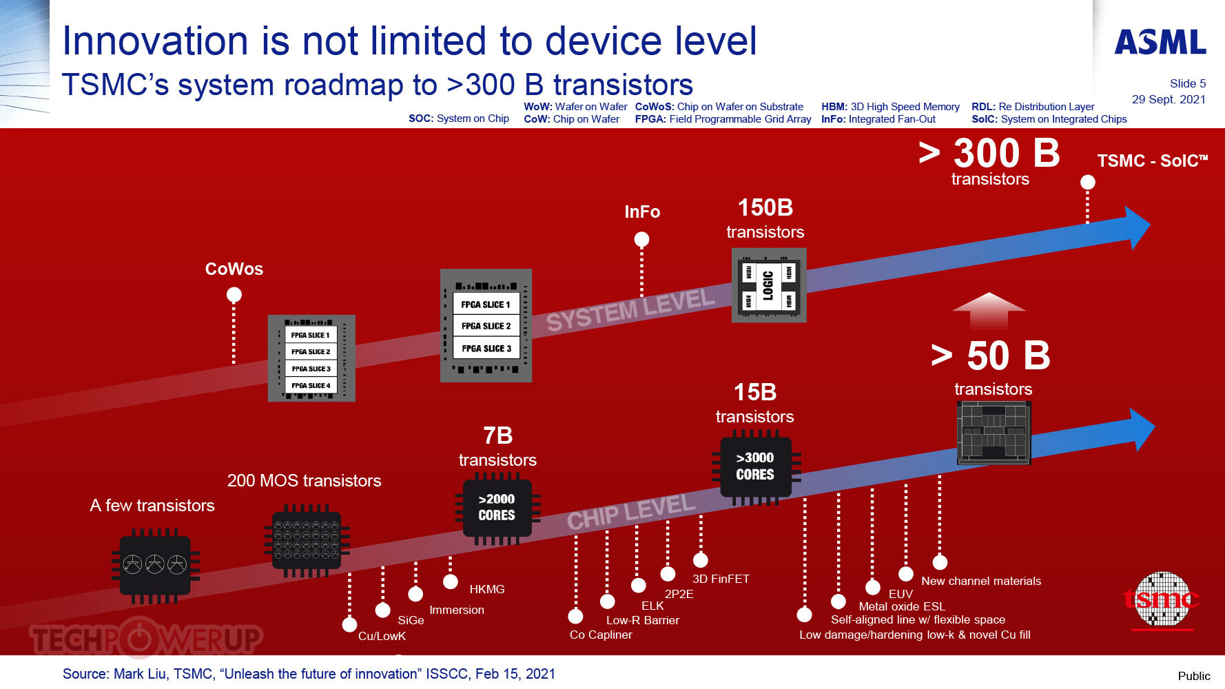
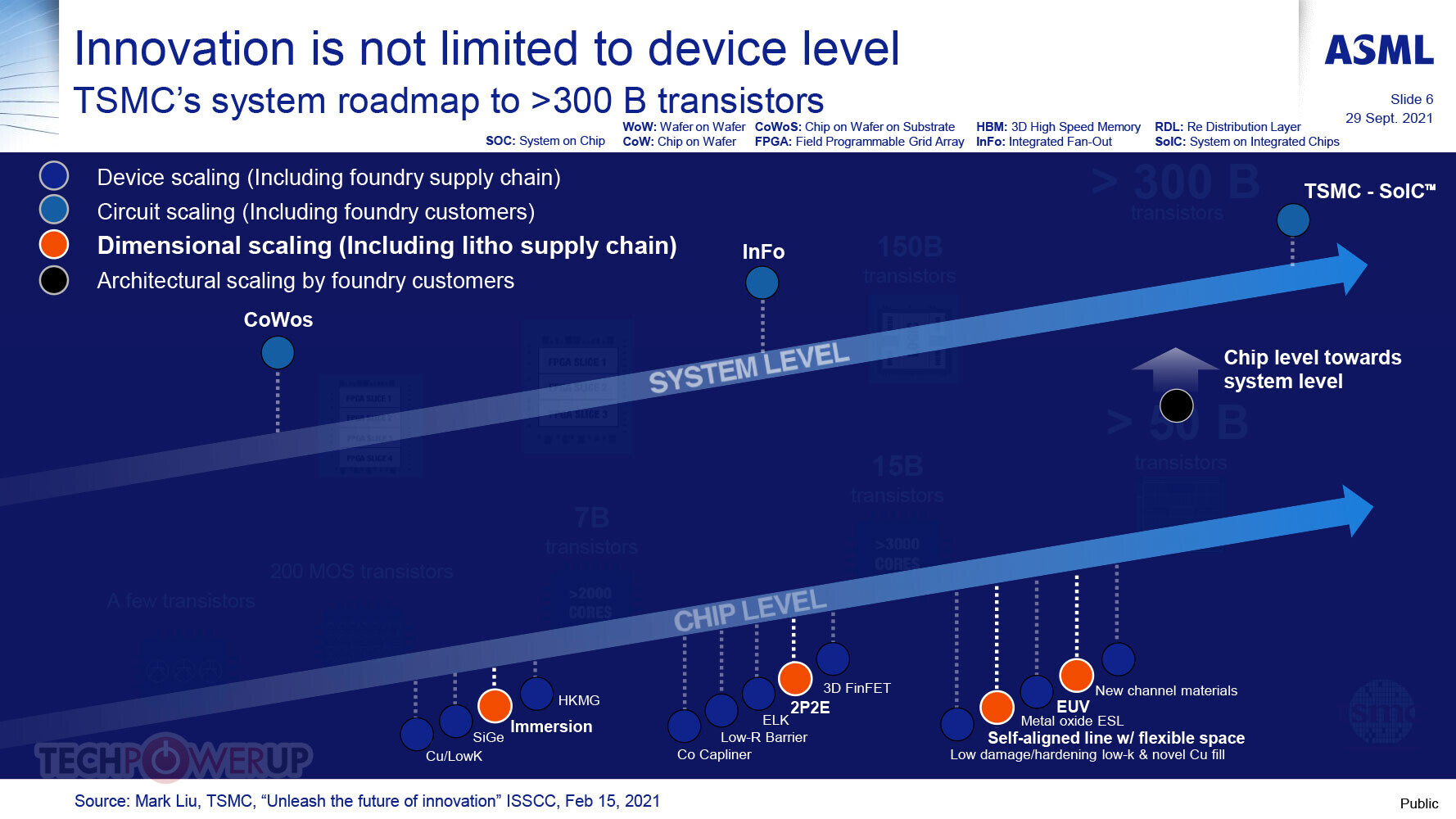
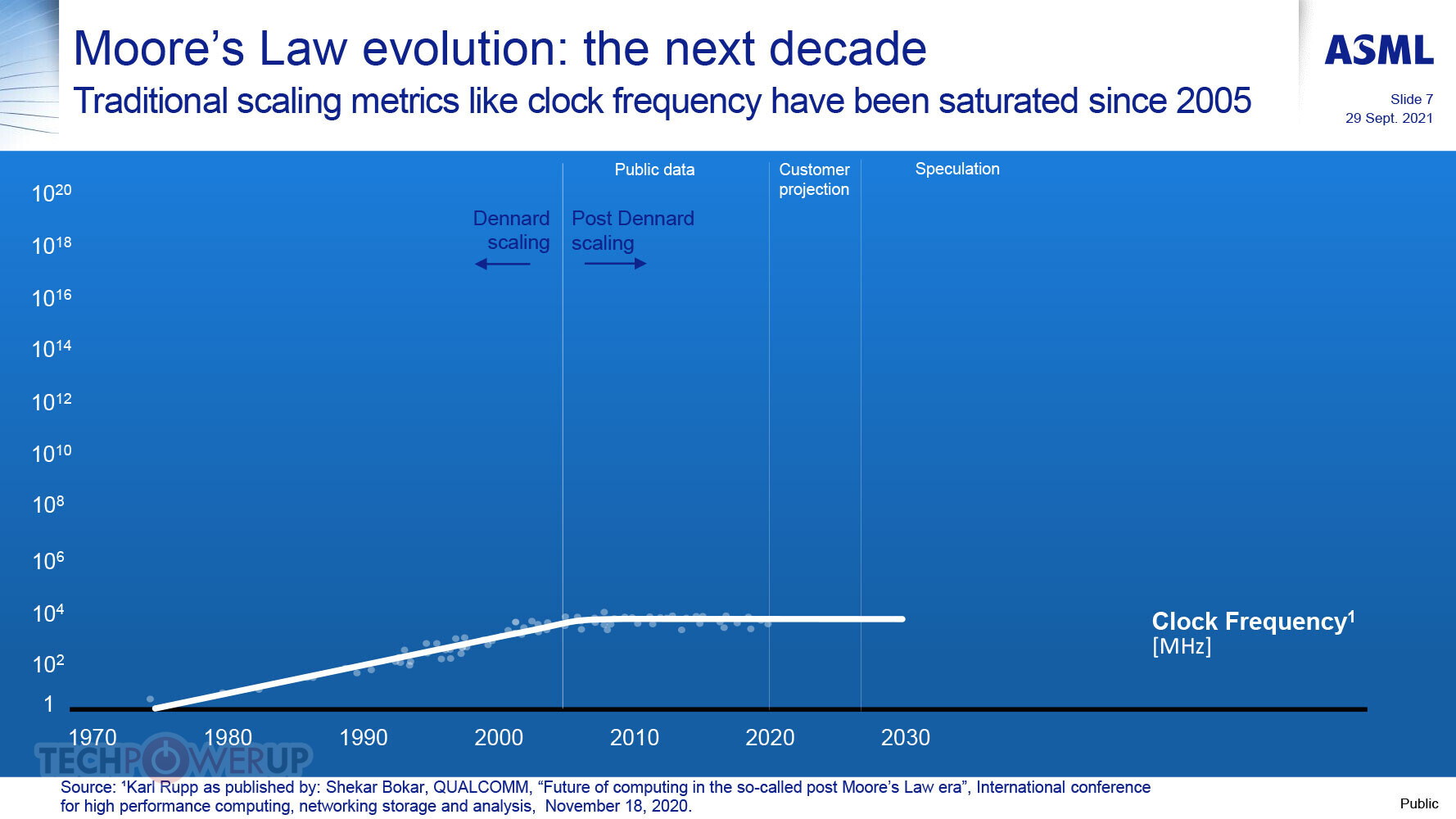
"Moore's Law is alive and well," says ASML, in its vision document addressing investors. The company manufactures the machines that perform the actual task of silicon lithography—turning silicon discs into wafers of logic or storage chips. It highlighted the various technologies making progress, which will help its semiconductor-fabrication customers, such as TSMC and their hundreds of clients, sustain Moore's Law all the way through this decade. The company predicts SoCs with as many as 300 billion transistors by 2030. To achieve this, the company is innovating in two distinct directions—at the chip-level, to increase transistor density per chip to over 50 billion transistors; and at the system level, through packaging technology innovations, to reach that ultimate transistor count.
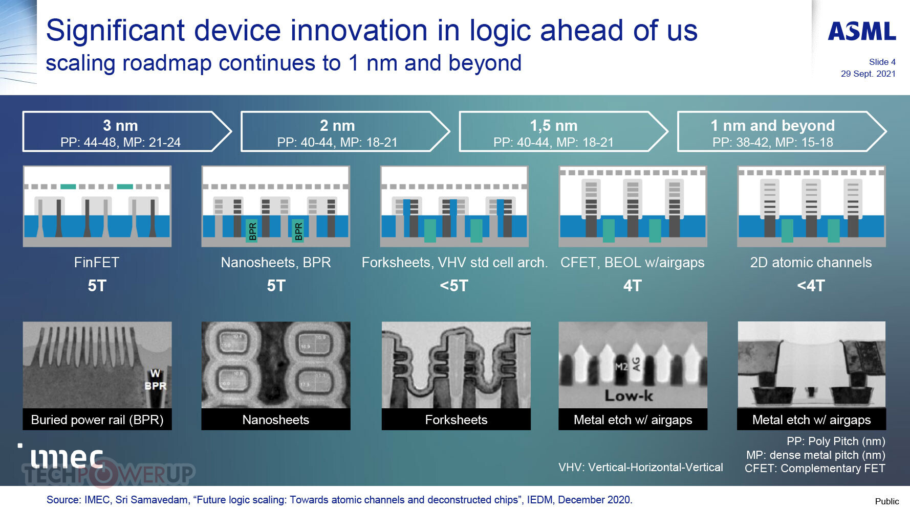
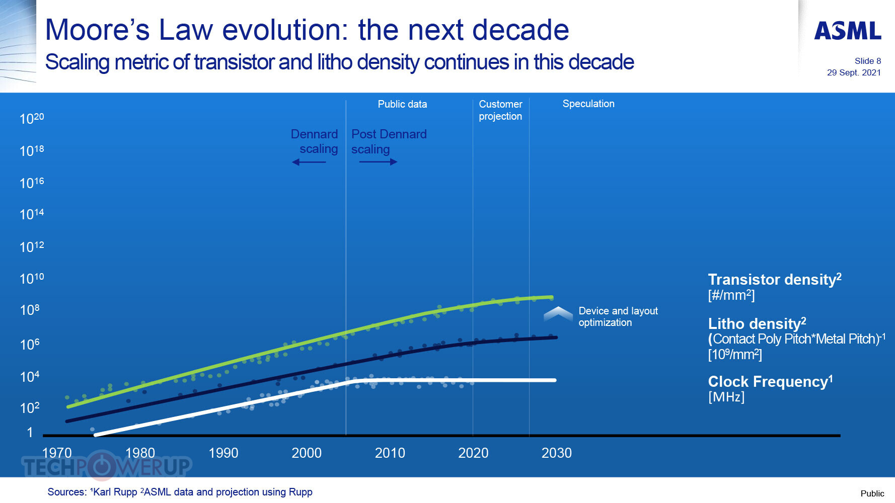
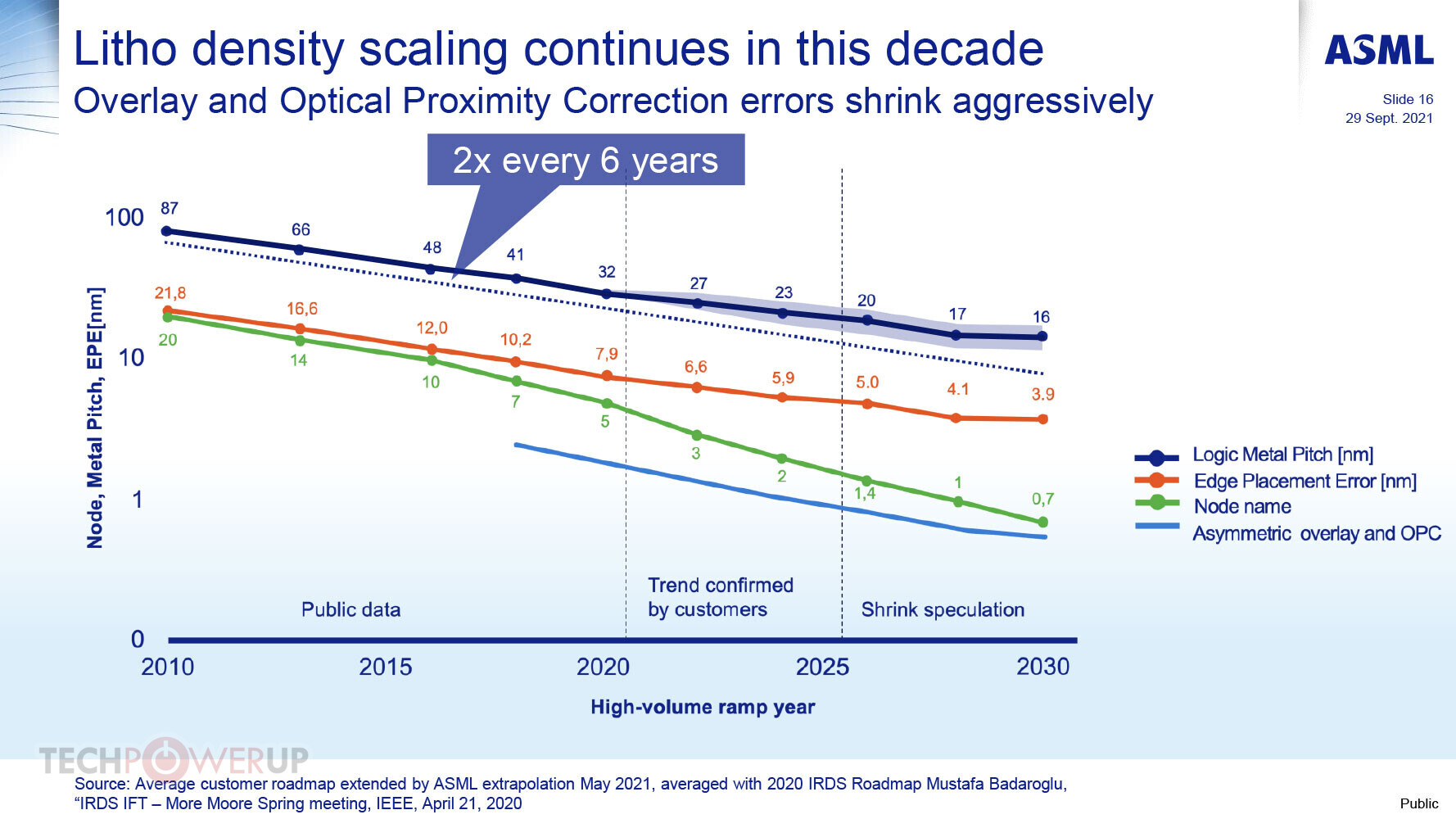
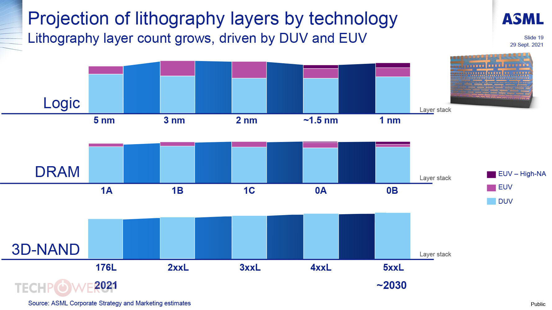
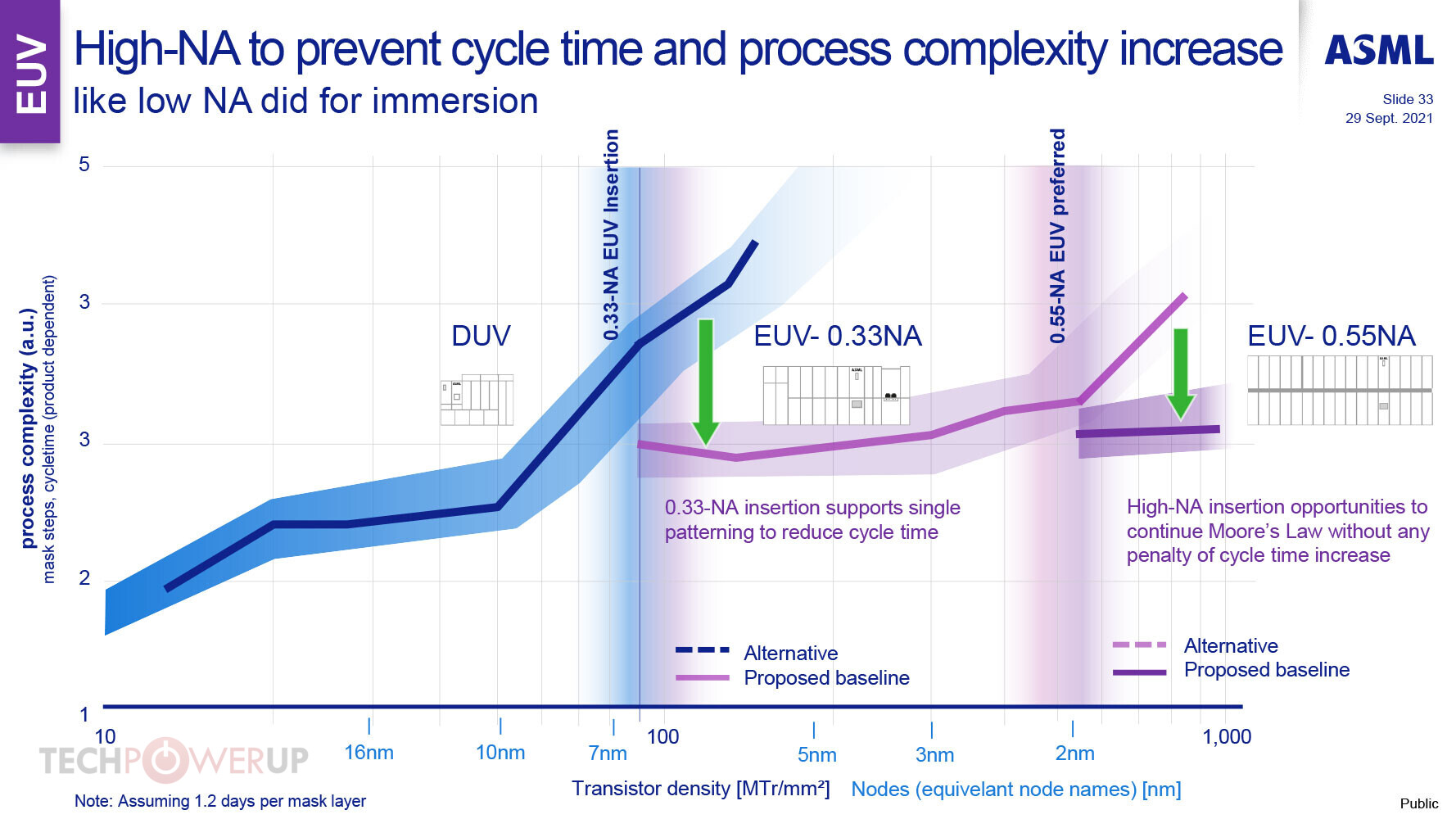
According to ASML's roadmap, at the turn of the decade, its technology enables 5 nm-class in production, and is at the cusp of a major breakthrough, nanosheet-FETs. which pave the way for 3 nm and 2 nm nodes, backed by EUV lithography. The journey from 2 nm to 1.5 nm will require another breakthrough, forked-nanosheets, and from 1.5 nm to 1 nm yet another breakthrough, CFET. Sub-1 nm fabrication will be possible toward the turn of this decade, thanks to 2D atomic channel technology, which is how chip-designers will be able to cram over 50 billion transistors per chip, and build MCM systems with over 300 billion transistors. The presentation predicts that besides 3D packaging, stacked silicon will also play a role, with multiple stacked logic layers, heterogenous chips with logic, storage, and I/O layers, stacked DRAM (up from single-digit layers to double-digits; and for NAND flash to grow from the current 176-layer, to nearly 500-layer by 2030.


 The complete slide-deck follows.


According to ASML's roadmap, at the turn of the decade, its technology enables 5 nm-class in production, and is at the cusp of a major breakthrough, nanosheet-FETs. which pave the way for 3 nm and 2 nm nodes, backed by EUV lithography. The journey from 2 nm to 1.5 nm will require another breakthrough, forked-nanosheets, and from 1.5 nm to 1 nm yet another breakthrough, CFET. Sub-1 nm fabrication will be possible toward the turn of this decade, thanks to 2D atomic channel technology, which is how chip-designers will be able to cram over 50 billion transistors per chip, and build MCM systems with over 300 billion transistors. The presentation predicts that besides 3D packaging, stacked silicon will also play a role, with multiple stacked logic layers, heterogenous chips with logic, storage, and I/O layers, stacked DRAM (up from single-digit layers to double-digits; and for NAND flash to grow from the current 176-layer, to nearly 500-layer by 2030.


9 Comments on Fabricating the Fabs: ASML Vision Document Predicts 300 Billion-Transistor Logic by 2030
Though, to be honest, I'm still surprised that the fab companies are able to make transistors as small as they are today.
*Because everything between CPU
registersexecution units and persistent storage is cache.Generally speaking thats seems little slower compared to the speeds TSMC and Samsung is moving
since we are in 5nm in 2021, possibly 4nm in 2022,3nm in 2023.