Wednesday, February 11th 2009

Intel Presents 32 nm Westmere Family of Processors
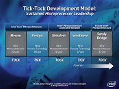
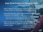
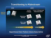
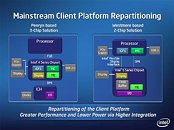
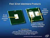
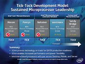
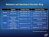
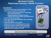
Intel today spread opens its plans to deal with the mainstream and value markets using its Nehalem micro-architecture. The company introduced to the media and analysts, its plans concerning the upcoming Westmere family of processors, a term used to describe Intel processors built using the company's 32 nm second-generation high-K silicon fabrication technology, while being based on the Nehalem micro-architecture. The presentation demystifies all confusion surrounding the company canning plans of dual-core 45 nm Nehalem-derivatives. The presentation also sheds light on what approach Intel plans to adopt with bringing the new architecture to the enterprise segment.Westmere and its rather speedy introduction (starting 2H 2009) shows that the company fast-tracked making the new 32 nm process operational. The new process makes the company ready to cater to large demands while minimizing production costs to the extant feasible. This can be noted from the recent expose of the Clarkdale and Arrandale chips that use portions of both 45 nm and 32 nm silicon technologies to fabricate different parts of the processor, taking advantage of the modular design of the chips. Intel also listed out roadmaps of both its client and enterprise platforms.Intel also added a brief note on the processors' security features that include new AES extensions that streamline security, minimizing the expense of data security on CPU time. The increase in transistor count over its previous generation processor (45 nm Penryn) enables Intel to expand the SIMD instruction-set beyond SSE 4.1 on Penryn (presumably with SSE 4.2 already found on Core i7). Intel also notes continued market and technology leadership for over three successive sub-generations of processors.





10 Comments on Intel Presents 32 nm Westmere Family of Processors
All I want to know is if sandy bridge will work with LGA1366. That would be awesomeness.
Damn this stuff gets old quick tho! My HD4850 is already seeming dated!
As far as making it smaller, they will continue, AFIK Intel hasn't even started to use the immersion lithography process, something that costs them on both ends. Currently IBM/AMD are using it for their fast transition to lower size fabs, and also the reason they have such low leakage for the Phenom II,it is a much cleaner process.