Report an Error


NVIDIA G70
G70

GF-7800-GT-A2

GF-7800-GTX-A2

GF-7800-GTX-512-A2

GF-7800-U-A2

QDFX-4500-N-A2
SIC66SIC66
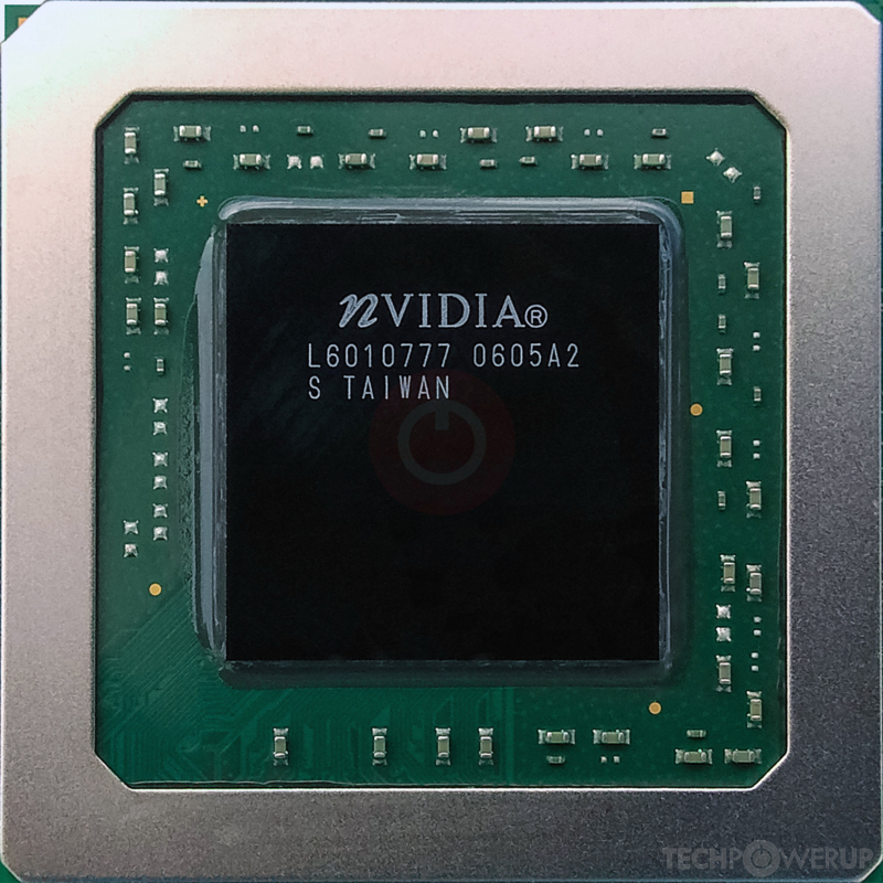
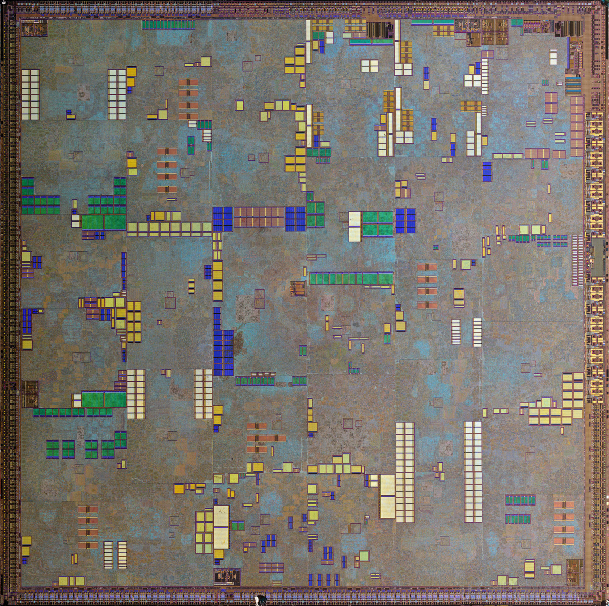
Die Shot

Block Diagram
NVIDIA's G70 GPU uses the Curie architecture and is made using a 110 nm production process at TSMC. With a die size of 333 mm² and a transistor count of 302 million it is a large chip. G70 supports DirectX 9.0c (Feature Level 9_3). For GPU compute applications, OpenCL version N/A can be used. It features 24 pixel shaders and 8 vertex shaders, 24 texture mapping units and 16 ROPs. Due to the lack of unified shaders you will not be able to run recent games at all (which require unified shader/DX10+ support).
Graphics Processor
- Released
- Jun 22nd, 2005
- GPU Name
- G70
- Codename
- NV47
- Architecture
- Curie
- Foundry
- TSMC
- Process Size
- 110 nm
- Transistors
- 302 million
- Density
- 906.9K / mm²
- Die Size
- 333 mm²
- Package
- FCBGA-1148
- Package Size
- 37.5mm x 37.5mm
Graphics Features
- DirectX
- 9.0c (9_3)
- OpenGL
- 2.1
- OpenCL
- N/A
- Vulkan
- N/A
- Shader Model
- 3.0
- WDDM
- 1.0
- PureVideo HD
- VP1
- VDPAU
- No Support
Render Config
- Pixel Shaders
- 24
- Vertex Shaders
- 8
- TMUs
- 24
- ROPs
- 16
- Max. TDP
- 108 W
- Tex L1 Cache
- 16 KB per 4 PS
- Tex L2 Cache
- 32 KB per 4 PS
All Curie GPUs
NVIDIA GPU Architecture History
- 2024 Blackwell
- 2023 Hopper
- 2022-2024 Ada Lovelace
- 2020-2024 Ampere
- 2018-2022 Turing
- 2017-2020 Volta
- 2016-2021 Pascal
- 2014-2019 Maxwell 2.0
- 2014-2017 Maxwell
- 2013-2015 Kepler 2.0
- 2012-2018 Kepler
- 2010-2016 Fermi 2.0
- 2010-2013 VLIW Vec4
- 2010-2016 Fermi
- 2007-2013 Tesla 2.0
- 2006-2010 Tesla
- 2003-2013 Curie
- 2003-2005 Rankine
- 2001-2003 Kelvin
- 1999-2005 Celsius
- 1998-2000 Fahrenheit
Graphics cards using the NVIDIA G70 GPU
| Name | Chip | Memory | Shaders | TMUs | ROPs | GPU Clock | Memory Clock |
|---|---|---|---|---|---|---|---|
| GF-7800-GT-A2 | 256 MB | 20 / 7 | 20 | 16 | 400 MHz | 500 MHz | |
| GF-7800-GTX-A2 | 256 MB | 24 / 8 | 24 | 16 | 430 MHz | 600 MHz | |
| GF-7800-GTX-512-A2 | 512 MB | 24 / 8 | 24 | 16 | 500 MHz | 800 MHz | |
| 512 MB | 24 / 8 | 24 | 16 | 470 MHz | 525 MHz | ||
| QDFX-4500-N-A2 | 512 MB | 24 / 8 | 24 | 16 | 430 MHz | 525 MHz | |
| 512 MB | 24 / 8 | 24 | 16 | 430 MHz | 525 MHz | ||
| 512 MB | 24 / 8 | 24 | 16 | 440 MHz | 550 MHz | ||
| 256 MB | 16 / 6 | 16 | 16 | 400 MHz | 550 MHz | ||
| GF-7800-GT-A2 | 256 MB | 20 / 7 | 20 | 16 | 400 MHz | 500 MHz | |
| GF-7800-GT-A2 | 256 MB | 16 / 6 | 16 | 8 | 375 MHz | 600 MHz | |
| GF-7800-GT-A2 | 512 MB | 20 / 7 | 20 | 16 | 425 MHz | 625 MHz | |
| GF-7800-GT-A2 | 512 MB | 24 / 8 | 24 | 16 | 425 MHz | 625 MHz |


G70 GPU Notes
| PureVideo HD: VP1 VDPAU: No Support Latest Drivers: Windows 2000: ForceWare Release 93.71 / 93.81 Beta Quadro Release 261.19 Windows XP / Server 2003 x64: GeForce Release 307.83 Quadro Release R310 U7 (312.69) Windows Vista / 7 / 8: GeForce Release 309.08 Quadro Release R310 U7 (312.69) |
Jun 11th, 2024 01:09 EDT
change timezone
Latest GPU Drivers
New Forum Posts
- Simple measurement of RADIATOR PERFORMANCE (61)
- Upgrading advice on the new AMD Processors coming out.... (27)
- VMware Workstation is now free for personal use (14)
- What do you mostly use your desktop PC for? (Pick your top 3!) (41)
- Memory Clock reported by GPU-Z and Nvidia performance overlay. (8)
- What's your latest tech purchase? (20754)
- RTX 4090 Won't Undervolt via Power Limit Slider?? (5)
- PC doesn't turn on or instantly turns off. (10)
- How we ended with 16x9 Aspect ratios (6)
- 49" AOC Gaming AG493QCX with remote. 3840 x 1080. 32:9. 144hz. (1)
Popular Reviews
- Pulsar Xlite V3 Review
- Intel Lunar Lake Technical Deep Dive - So many Revolutions in One Chip
- Upcoming Hardware Launches 2024 (Updated May 2024)
- NZXT H6 Flow RGB Review
- AMD Ryzen 7 7800X3D Review - The Best Gaming CPU
- AQIRYS HYDRA 360 AIO Review
- Quick Look: Final UX2000 Wireless Noise Canceling Headphones
- Ghost of Tsushima Performance Benchmark Review - 35 GPUs Tested
- Thermal Grizzly KryoSheet Review - Tested on RX 7900 XTX with 475 W
- ASUS Radeon RX 7900 GRE TUF OC Review
Controversial News Posts
- AMD RDNA 5 a "Clean Sheet" Graphics Architecture, RDNA 4 Merely Corrects a Bug Over RDNA 3 (145)
- NVIDIA RTX 5090 "Blackwell" Founders Edition to Implement the "RTX 4090 Ti" Cinderblock Design (118)
- AMD Zen 5 Storms into Gaming Desktops with Ryzen 9000 "Granite Ridge" Processors (100)
- Biden Administration to Revive Trump-Era Tariffs on China-made GPUs and Motherboards (95)
- ASRock Innovates First AMD Radeon RX 7000 Graphics Card with 12V-2x6 Power Connector (94)
- AMD Ryzen 9000 Zen 5 Single Thread Performance at 5.80 GHz Found 19% Over Zen 4 (92)
- Nightmare Fuel for Intel: Arm CEO Predicts Arm will Take Over 50% Windows PC Market-share by 2029 (91)
- AMD Ryzen 9000 Zen 5 "Granite Ridge" Desktop Processors Launch Late-July (83)