Report an Error


NVIDIA G73

G73
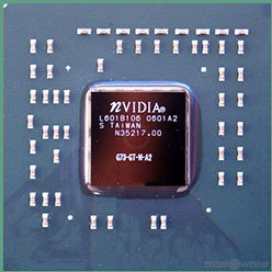
G73-GT-N-A2

G73M-U-N-A2

G73 BGA

SIC66SIC66
Die Shot
NVIDIA's G73 GPU uses the Curie architecture and is made using a 90 nm production process at TSMC. With a die size of 125 mm² and a transistor count of 177 million it is a small chip. G73 supports DirectX 9.0c (Feature Level 9_3). For GPU compute applications, OpenCL version N/A can be used. It features 12 pixel shaders and 5 vertex shaders, 12 texture mapping units and 8 ROPs. Due to the lack of unified shaders you will not be able to run recent games at all (which require unified shader/DX10+ support).
Graphics Processor
- Released
- Mar 1st, 2006
- GPU Name
- G73
- Codename
- NV4B
- Architecture
- Curie
- Foundry
- TSMC
- Process Size
- 90 nm
- Transistors
- 177 million
- Density
- 1.4M / mm²
- Die Size
- 125 mm²
- Package
- BGA-820
Graphics Features
- DirectX
- 9.0c (9_3)
- OpenGL
- 2.1
- OpenCL
- N/A
- Vulkan
- N/A
- Shader Model
- 3.0
- WDDM
- 1.0
- PureVideo HD
- VP1
- VDPAU
- No Support
Render Config
- Pixel Shaders
- 12
- Vertex Shaders
- 5
- TMUs
- 12
- ROPs
- 8
- Max. TDP
- 40 W
- Tex L1 Cache
- 16 KB per 4 PS
- Tex L2 Cache
- 32 KB per 4 PS
All Curie GPUs
NVIDIA GPU Architecture History
- 2024 Blackwell
- 2023 Hopper
- 2022-2024 Ada Lovelace
- 2020-2024 Ampere
- 2018-2022 Turing
- 2017-2020 Volta
- 2016-2021 Pascal
- 2014-2019 Maxwell 2.0
- 2014-2017 Maxwell
- 2013-2015 Kepler 2.0
- 2012-2018 Kepler
- 2010-2016 Fermi 2.0
- 2010-2013 VLIW Vec4
- 2010-2016 Fermi
- 2007-2013 Tesla 2.0
- 2006-2010 Tesla
- 2003-2013 Curie
- 2003-2005 Rankine
- 2001-2003 Kelvin
- 1999-2005 Celsius
- 1998-2000 Fahrenheit
Graphics cards using the NVIDIA G73 GPU
| Name | Chip | Memory | Shaders | TMUs | ROPs | GPU Clock | Memory Clock |
|---|---|---|---|---|---|---|---|
| 128 MB | 12 / 5 | 12 | 8 | 350 MHz | 600 MHz | ||
| QD-NVS-300M-N-A2 | 256 MB | 8 / 4 | 8 | 8 | 500 MHz | 700 MHz | |
| GF-GO7600-N-A2 | 256 MB | 8 / 4 | 8 | 8 | 450 MHz | 350 MHz | |
| 128 MB | 12 / 5 | 12 | 8 | 450 MHz | 500 MHz | ||
| 256 MB | 12 / 5 | 12 | 8 | 350 MHz | 333 MHz | ||
| G73-GT-N-A2 | 128 MB | 8 / 4 | 8 | 8 | 350 MHz | 500 MHz | |
| G73-GT-N-A2 | 256 MB | 12 / 5 | 12 | 8 | 560 MHz | 700 MHz | |
| 128 MB | 8 / 4 | 8 | 8 | 350 MHz | 325 MHz |


G73 GPU Notes
| PureVideo HD: VP1 VDPAU: No Support Latest Drivers: Windows 2000: ForceWare Release 93.71 / 93.81 Beta Quadro Release 261.19 Windows XP / Server 2003 x64: GeForce Release 307.83 Quadro Release R310 U7 (312.69) Windows Vista / 7 / 8: GeForce Release 309.08 Quadro Release R310 U7 (312.69) |
May 29th, 2024 07:49 EDT
change timezone
Latest GPU Drivers
New Forum Posts
- Dell T7810 workstation standard power supply??? (25)
- Browser Bechmark scores (104)
- Do you use Linux? (284)
- What's your latest tech purchase? (20691)
- Poor thermals w/ Lian Li A4-H2O (1)
- Msi 4070 started getting nvlddmkm.sys Black Screen/ Freeze after months of healty usege (0)
- Performance testing: setting image src attributes dynamically (6)
- Post Your TIMESPY, PCMARK10 & FIRESTRIKE SCORES! (2019) (247)
- Post your Final Fantasy XV Benchmark Results (962)
- 2022-X58/1366 PIN Motherboards NVME M.2 SSD BIOS MOD Collection (693)
Popular Reviews
- Upcoming Hardware Launches 2024 (Updated May 2024)
- Lian Li O11 Dynamic EVO XL Review
- Senua’s Saga: Hellblade II: DLSS vs. FSR vs. XeSS Comparison Review
- Montech Titan Gold 1000 W Review
- Senua's Saga: Hellblade II Performance Benchmark Review
- Waizowl OGM Cloud Review
- Ghost of Tsushima Performance Benchmark Review - 35 GPUs Tested
- Montech HyperFlow ARGB 240 AIO Review
- Ghost of Tsushima: DLSS vs. FSR vs. XeSS Comparison Review
- AMD Ryzen 7 7800X3D Review - The Best Gaming CPU
Controversial News Posts
- AMD to Redesign Ray Tracing Hardware on RDNA 4 (227)
- NVIDIA to Only Launch the Flagship GeForce RTX 5090 in 2024, Rest of the Series in 2025 (154)
- AMD Hits Highest-Ever x86 CPU Market Share in Q1 2024 Across Desktop and Server (140)
- AMD RDNA 5 a "Clean Sheet" Graphics Architecture, RDNA 4 Merely Corrects a Bug Over RDNA 3 (139)
- NVIDIA RTX 5090 "Blackwell" Founders Edition to Implement the "RTX 4090 Ti" Cinderblock Design (108)
- AMD Ryzen 9 7900X3D Now at a Mouth-watering $329 (104)
- Core Configurations of Intel Core Ultra 200 "Arrow Lake-S" Desktop Processors Surface (101)
- Biden Administration to Revive Trump-Era Tariffs on China-made GPUs and Motherboards (95)