Report an Error


NVIDIA GF104

GF104

GF104-300-KA-A1

N12E-GTX-A1
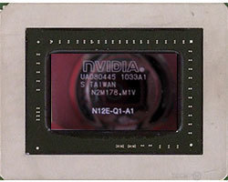
N12E-Q1-A1

N12E-Q3-A1
Block Diagram

SM Diagram
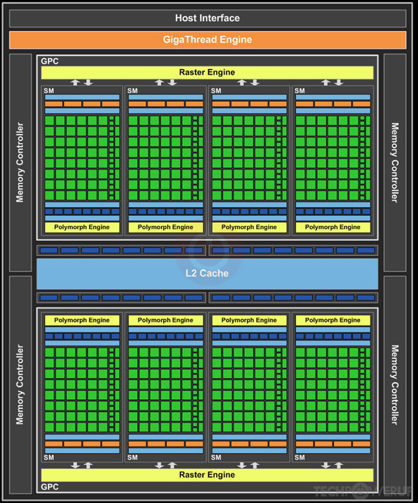
NVIDIA's GF104 GPU uses the Fermi architecture and is made using a 40 nm production process at TSMC. With a die size of 332 mm² and a transistor count of 1,950 million it is a large chip. GF104 supports DirectX 12 (Feature Level 11_0). For GPU compute applications, OpenCL version 1.1 and CUDA 2.1 can be used. It features 384 shading units, 64 texture mapping units and 32 ROPs.
Further reading:
Fermi Compute Architecture 
Graphics Processor
- Released
- Jul 12th, 2010
- GPU Name
- GF104
- Codename
- NVC4
- Architecture
- Fermi
- Foundry
- TSMC
- Process Size
- 40 nm
- Transistors
- 1,950 million
- Density
- 5.9M / mm²
- Die Size
- 332 mm²
- Package
- BGA-1724
Graphics Features
- DirectX
- 12 (11_0)
- OpenGL
- 4.6
- OpenCL
- 1.1
- Vulkan
- N/A
- CUDA
- 2.1
- Shader Model
- 5.1
- WDDM
- 2.3
- PureVideo HD
- VP4
- VDPAU
- Feature Set C
Render Config
- Shading Units
- 384
- TMUs
- 64
- ROPs
- 32
- SM Count
- 8
- SFUs
- 64
- GPCs
- 2
- L1 Cache
- 64 KB per SM
- L2 Cache
- 512 KB
- Max. TDP
- 160 W
All Fermi GPUs
- NVIDIA EXMF104
- NVIDIA GF100
- NVIDIA GF104
- NVIDIA GF106
- NVIDIA GF108
NVIDIA GPU Architecture History
- 2024 Blackwell
- 2023 Hopper
- 2022-2024 Ada Lovelace
- 2020-2024 Ampere
- 2018-2022 Turing
- 2017-2020 Volta
- 2016-2021 Pascal
- 2014-2019 Maxwell 2.0
- 2014-2017 Maxwell
- 2013-2015 Kepler 2.0
- 2012-2018 Kepler
- 2010-2016 Fermi 2.0
- 2010-2013 VLIW Vec4
- 2010-2016 Fermi
- 2007-2013 Tesla 2.0
- 2006-2010 Tesla
- 2003-2013 Curie
- 2003-2005 Rankine
- 2001-2003 Kelvin
- 1999-2005 Celsius
- 1998-2000 Fahrenheit
Graphics cards using the NVIDIA GF104 GPU
| Name | Chip | Memory | Shaders | TMUs | ROPs | GPU Clock | Memory Clock |
|---|---|---|---|---|---|---|---|
| GF104-325-A1 | 1024 MB | 336 | 56 | 32 | 675 MHz | 900 MHz | |
| GF104-225-A1 | 1024 MB | 288 | 48 | 32 | 650 MHz | 850 MHz | |
| N12E-GTX-A1 | 2 GB | 384 | 64 | 32 | 575 MHz | 750 MHz | |
| N12E-Q3-A1 | 2 GB | 336 | 56 | 32 | 475 MHz | 625 MHz | |
| N12E-Q1-A1 | 2 GB | 240 | 40 | 32 | 450 MHz | 625 MHz | |
| N11E-GT | 1536 MB | 288 | 48 | 24 | 535 MHz | 750 MHz | |
| GF104-325-A1 | 1024 MB | 336 | 56 | 32 | 650 MHz | 850 MHz | |
| GF104-300-KB-A1 | 1024 MB | 336 | 56 | 32 | 701 MHz | 900 MHz | |
| GF104-300-KB-A1 | 768 MB | 336 | 56 | 24 | 675 MHz | 900 MHz |


GF104 GPU Notes
| PureVideo HD: VP4 VDPAU: Feature Set C |
May 21st, 2024 13:59 EDT
change timezone
Latest GPU Drivers
New Forum Posts
- TPU's Rosetta Milestones and Daily Pie Thread (1892)
- Win11 24H2 Issue (2)
- Post Your TIMESPY, PCMARK10 & FIRESTRIKE SCORES! (2019) (224)
- Cooling 7800X3D with Thermalright Phantom Spirit EVO and idle temp is around 60c. Is this normal? (10)
- Would a ag620 hold a 5700x3d in stock settings? (12)
- What's your latest tech purchase? (20614)
- Ryzen 5 5600x stock overclocked reaching high temps (23)
- Post your Cinebench 2024 score (463)
- Kepler BIOS Tweaker problem (15)
- Post your cooling. (0)
Popular Reviews
- Ghost of Tsushima Performance Benchmark Review - 35 GPUs Tested
- Ghost of Tsushima: DLSS vs. FSR vs. XeSS Comparison Review
- PNY XLR8 Gaming EPIC-X RGB DDR5-6400 CL32 32 GB Review
- TerraMaster D8 Hybrid Review
- Silverstone Shark Force 120 mm Fan Review
- Homeworld 3 Performance Benchmark Review - 35 GPUs Tested
- Upcoming Hardware Launches 2023 (Updated Feb 2024)
- Lofree Edge Ultra-Low Profile Wireless Mechanical Keyboard Review
- AMD Ryzen 7 7800X3D Review - The Best Gaming CPU
- AMD Ryzen 7 7700 Review - Affordable Zen 4 Powerhouse
Controversial News Posts
- Intel Statement on Stability Issues: "Motherboard Makers to Blame" (269)
- AMD to Redesign Ray Tracing Hardware on RDNA 4 (227)
- Windows 11 Now Officially Adware as Microsoft Embeds Ads in the Start Menu (173)
- NVIDIA to Only Launch the Flagship GeForce RTX 5090 in 2024, Rest of the Series in 2025 (154)
- AMD Hits Highest-Ever x86 CPU Market Share in Q1 2024 Across Desktop and Server (140)
- AMD RDNA 5 a "Clean Sheet" Graphics Architecture, RDNA 4 Merely Corrects a Bug Over RDNA 3 (139)
- AMD's RDNA 4 GPUs Could Stick with 18 Gbps GDDR6 Memory (114)
- AMD Ryzen 9 7900X3D Now at a Mouth-watering $329 (104)