Report an Error


NVIDIA Quadro P1000
- Graphics Processor
- GP107
- Cores
- 640
- TMUs
- 40
- ROPs
- 32
- Memory Size
- 4 GB
- Memory Type
- GDDR5
- Bus Width
- 128 bit


GPU
I/O
Recommended Gaming Resolutions:
- 1600x900
- 1920x1080
- 2560x1440
The Quadro P1000 was a professional graphics card by NVIDIA, launched on February 7th, 2017. Built on the 14 nm process, and based on the GP107 graphics processor, in its GP107-860-A1 variant, the card supports DirectX 12. The GP107 graphics processor is an average sized chip with a die area of 132 mm² and 3,300 million transistors. Unlike the fully unlocked GeForce GTX 1050 Ti, which uses the same GPU but has all 768 shaders enabled, NVIDIA has disabled some shading units on the Quadro P1000 to reach the product's target shader count. It features 640 shading units, 40 texture mapping units, and 32 ROPs. NVIDIA has paired 4 GB GDDR5 memory with the Quadro P1000, which are connected using a 128-bit memory interface. The GPU is operating at a frequency of 1266 MHz, which can be boosted up to 1480 MHz, memory is running at 1253 MHz (5 Gbps effective).
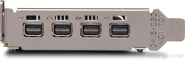
Being a single-slot card, the NVIDIA Quadro P1000 does not require any additional power connector, its power draw is rated at 47 W maximum. Display outputs include: 4x mini-DisplayPort 1.4a. Quadro P1000 is connected to the rest of the system using a PCI-Express 3.0 x16 interface. The card measures 150 mm in length, 69 mm in width, and features a single-slot cooling solution.
Being a single-slot card, the NVIDIA Quadro P1000 does not require any additional power connector, its power draw is rated at 47 W maximum. Display outputs include: 4x mini-DisplayPort 1.4a. Quadro P1000 is connected to the rest of the system using a PCI-Express 3.0 x16 interface. The card measures 150 mm in length, 69 mm in width, and features a single-slot cooling solution.
Graphics Processor
Graphics Card
- Release Date
- Feb 7th, 2017
- Generation
-
Quadro Pascal
(Px000)
- Predecessor
- Quadro Maxwell
- Successor
- Quadro Volta
- Production
- End-of-life
- Bus Interface
- PCIe 3.0 x16
Relative Performance
Based on TPU review data: "Performance Summary" at 1920x1080, 4K for 2080 Ti and faster.
Performance estimated based on architecture, shader count and clocks.
Clock Speeds
- Base Clock
- 1266 MHz
- Boost Clock
- 1480 MHz
- Memory Clock
-
1253 MHz
5 Gbps effective
Memory
- Memory Size
- 4 GB
- Memory Type
- GDDR5
- Memory Bus
- 128 bit
- Bandwidth
- 80.19 GB/s
Render Config
- Shading Units
- 640
- TMUs
- 40
- ROPs
- 32
- SM Count
- 5
- L1 Cache
- 48 KB (per SM)
- L2 Cache
- 1024 KB
Theoretical Performance
- Pixel Rate
- 47.36 GPixel/s
- Texture Rate
- 59.20 GTexel/s
- FP16 (half)
- 29.60 GFLOPS (1:64)
- FP32 (float)
- 1.894 TFLOPS
- FP64 (double)
- 59.20 GFLOPS (1:32)
Board Design
- Slot Width
- Single-slot
- Length
- 150 mm
5.9 inches
- Width
- 69 mm
2.7 inches
- TDP
- 47 W
- Suggested PSU
- 200 W
- Outputs
- 4x mini-DisplayPort 1.4a
- Power Connectors
- None
- Board Number
- PG212 SKU 502
Graphics Features
- DirectX
- 12 (12_1)
- OpenGL
- 4.6
- OpenCL
- 3.0
- Vulkan
- 1.3
- CUDA
- 6.1
- Shader Model
- 6.7
GP107 GPU Notes
| NVENC: 6th Gen NVDEC: 3rd Gen PureVideo HD: VP8 VDPAU: Feature Set H |
Retail boards based on this design (2)
| Name | GPU Clock | Boost Clock | Memory Clock | Other Changes |
|---|---|---|---|---|
| 1266 MHz | 1480 MHz | 1253 MHz | ||
| 1266 MHz | 1480 MHz | 1253 MHz |


May 17th, 2024 18:36 EDT
change timezone
Latest GPU Drivers
New Forum Posts
- AIO Water Cooler vs Tower Air Cooler (47)
- Radeon RX 6700, 6700 XT & 6750 XT users club (939)
- Safe to replace keycaps with new custom ones? (3)
- Razer Blade 18 Laptop / ThrottleStop not working :( (3)
- What are you playing? (20668)
- Ghost of Tsushima PC Port !!!! (51)
- ThrottleStop stopped working with Windows 23H2 update, VBS & virtualization disabled, BIOS rollback, no undervolt protection notice, what next? (3)
- not impressed - nvme vs ssd (136)
- Not getting the performance I should be with the components I have (2)
- LOL ASUS says this is $200 in repair, Steve from gamers Nexus smokes ASUS, Steam Deck til I die boys!!!! (108)
Popular Reviews
- Homeworld 3 Performance Benchmark Review - 35 GPUs Tested
- Ghost of Tsushima Performance Benchmark Review - 35 GPUs Tested
- Enermax REVOLUTION D.F. X 1200 W Review
- Lofree Edge Ultra-Low Profile Wireless Mechanical Keyboard Review
- Silverstone Shark Force 120 mm Fan Review
- Upcoming Hardware Launches 2023 (Updated Feb 2024)
- AMD Ryzen 7 7800X3D Review - The Best Gaming CPU
- ZMF Caldera Closed Planar Magnetic Headphones Review
- Corsair MP700 Pro SE 4 TB Review
- Horizon Forbidden West Performance Benchmark Review - 30 GPUs Tested
Controversial News Posts
- Intel Statement on Stability Issues: "Motherboard Makers to Blame" (268)
- AMD to Redesign Ray Tracing Hardware on RDNA 4 (227)
- Windows 11 Now Officially Adware as Microsoft Embeds Ads in the Start Menu (172)
- NVIDIA to Only Launch the Flagship GeForce RTX 5090 in 2024, Rest of the Series in 2025 (154)
- AMD Hits Highest-Ever x86 CPU Market Share in Q1 2024 Across Desktop and Server (138)
- AMD RDNA 5 a "Clean Sheet" Graphics Architecture, RDNA 4 Merely Corrects a Bug Over RDNA 3 (130)
- AMD's RDNA 4 GPUs Could Stick with 18 Gbps GDDR6 Memory (114)
- AMD Ryzen 9 7900X3D Now at a Mouth-watering $329 (104)