News Posts matching #16 nm

Return to Keyword Browsing

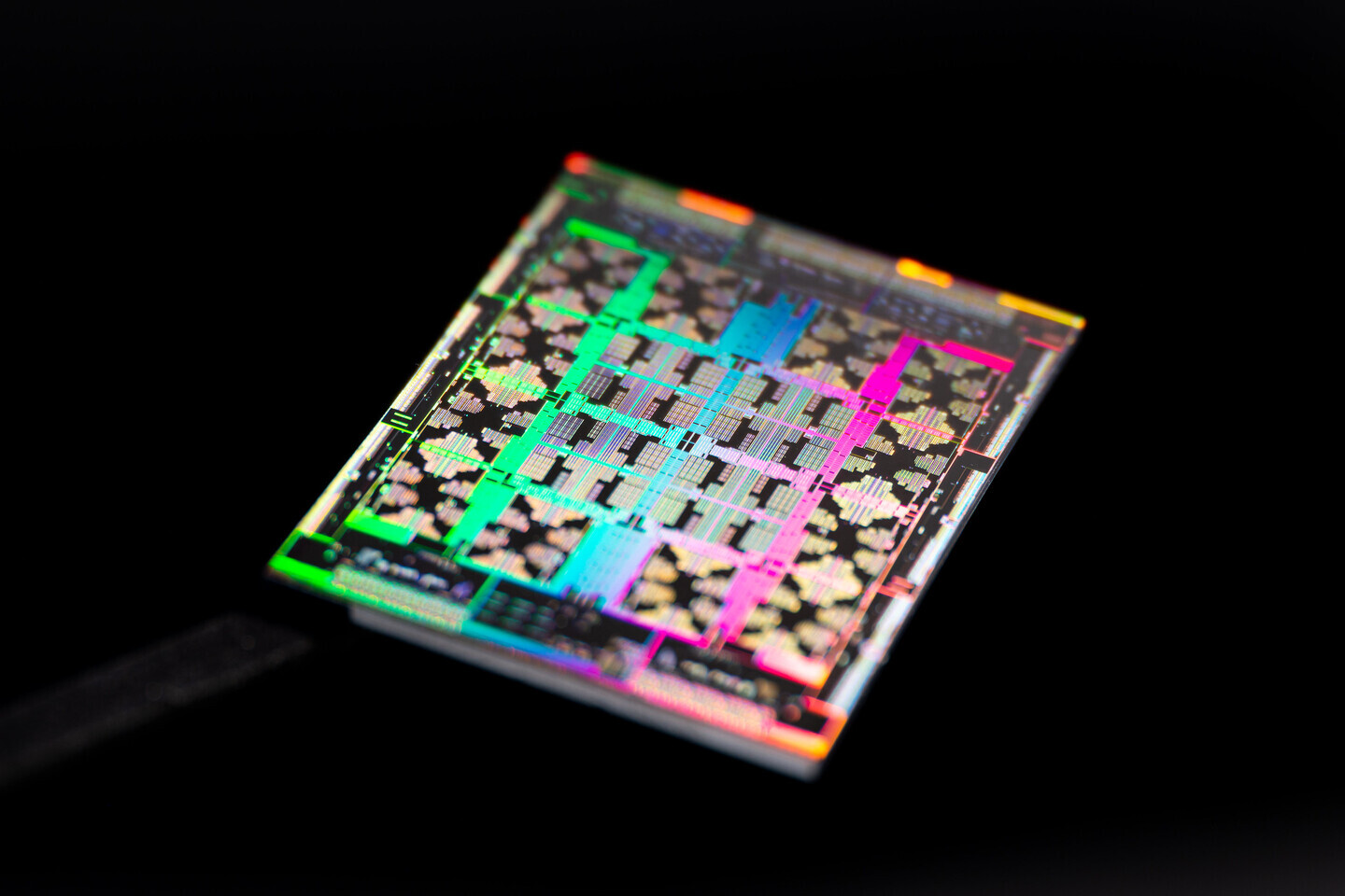
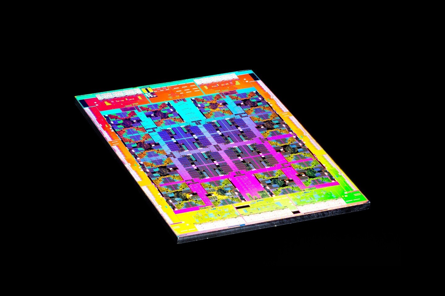
AMD Announces Spartan UltraScale+ Family of FPGAs

AMD today announced the AMD Spartan UltraScale+ FPGA family, the newest addition to the extensive portfolio of AMD Cost-Optimized FPGAs and adaptive SoCs. Delivering cost and power-efficient performance for a wide range of I/O-intensive applications at the edge, Spartan UltraScale+ devices offer the industry's highest I/O to logic cell ratio in FPGAs built in 28 nm and lower process technology, deliver up to 30 percent lower total power consumption versus the previous generation, and contain the most robust set of security features in the AMD Cost-Optimized Portfolio.

"For over 25 years the Spartan FPGA family has helped power some of humanity's finest achievements, from lifesaving automated defibrillators to the CERN particle accelerator advancing the boundaries of human knowledge," said Kirk Saban, corporate vice president, Adaptive and Embedded Computing Group, AMD. "Building on proven 16 nm technology, the Spartan UltraScale+ family's enhanced security and features, common design tools, and long product lifecycles further strengthen our market-leading FPGA portfolio and underscore our commitment to delivering cost-optimized products for customers."

Zhaoxin Launches KX-7000 Desktop 8-Core x86 Processor to Power China's Ambitions

After years of delays, Chinese chipmaker Zhaoxin has finally launched its long-awaited KX-7000 series consumer CPUs, only one of its kind in China, based on the licensed x86-64 ISA. Zhaoxin claims the new 8-core processors based on "Century Avenue" uArch deliver double the performance of previous generations. Leveraging architectural improvements and 4X more cache, the KX-7000 represents essential progress for China's domestic semiconductor industry. While still likely lagging behind rival AMD and Intel chips in raw speed, the KX-7000 matches competitive specs in areas like DDR5 memory, PCIe 4.0, and USB4 support. For Chinese efforts to attain technological independence, closing feature gaps with foreign processors is just as crucial as boosting performance. Manufactured on a 16 nm process, the KX-7000 does not use the best silicon node available.

Other chip details include out-of-order execution (OoOE), 24 PCIe 4.0 lanes, a 32 MB pool of L3 cache and 4 MB L2 cache, a base frequency of 3.2 GHz, and a boost clock of 3.7 GHz. Interestingly, the CPU also has VT-x, BT-d 2.5, SSE4.2/AVX/AVX2 support, most likely also licensed from the x86 makers Intel and/or AMD. Ultimately, surpassing Western processors is secondary for China next to attaining self-reliance. Instructions like SM encryption catering to domestic data protection priorities underscore how the KX-7000 advances strategic autonomy goals. With its x86 architecture license giving software compatibility and now a vastly upgraded platform, the KX-7000 will raise China's chip capabilities even if it is still trailing rivals' speeds. Ongoing progress closing that performance gap could position Zhaoxin as a mainstream alternative for local PC builders and buyers.

China's Share in Mature Process Capacity Predicted to Hit 29% in 2023, Climbing to 33% by 2027

TrendForce reports that from 2023 to 2027, the global ratio of mature (>28 nm) to advanced (<16 nm) processes is projected to hover around 7:3. Propelled by policies and incentives promoting local production and domestic IC development, China's mature process capacity is anticipated to grow from 29% this year to 33% by 2027. Leading the charge are giants like SMIC, HuaHong Group, and Nexchip, while Taiwan's share is estimated to consolidate from 49% down to 42%.

Expansion predominantly targets specialty processes such as Driver ICs, CIS/ISPs, and Power Discretes, with second and third-tier Taiwanese manufacturers at the forefront
Within the Driver IC sector, the spotlight is on high voltage (HV) specialty processes. As companies aggressively pursue the 40/28 nm HV process, UMC currently dominates, trailed by GlobalFoundries. Yet, SMIC's 28HV and Nexchip's 40HV are gearing up for mass production in 4Q23 and 1H24, respectively—narrowing their technological gap with other foundries. Notably, competitors with similar process capabilities and capacities, such as PSMC, and those without twelve-inch factories like Vanguard and DBHitek, are poised to face challenges head-on in the short term. This trend may also have long-term implications for UMC and GlobalFoundries.

Avicena Demonstrates First microLED Based Transceiver IC in 16 nm finFET CMOS for Chip-to-Chip Communications

Avicena, a privately held company headquartered in Sunnyvale, CA, is demonstrating its LightBundle multi-Tbps chip-to-chip interconnect technology at the European Conference for Optical Communications (ECOC) 2023 in Glasgow, Scotland (https://www.ecocexhibition.com/). Avicena's microLED-based LightBundle architecture breaks new ground by unlocking the performance of processors, memory and sensors, removing key bandwidth and proximity constraints while simultaneously offering class leading energy efficiency.

"As generative AI continues to evolve, the role of high bandwidth-density, low-power and low latency interconnects between xPUs and HBM modules cannot be overstated", says Chris Pfistner, VP Sales & Marketing of Avicena. "Avicena's innovative LightBundle interconnects have the potential to fundamentally change the way processors connect to each other and to memory because their inherent parallelism is well-matched to the internal wide and slow bus architecture within ICs. With a roadmap to multi-terabit per second capacity and sub-pJ/bit efficiency these interconnects are poised to enable the next era of AI innovation, paving the way for even more capable models and a wide range of AI applications that will shape the future."

Winbond Introduces Innovative CUBE Architecture for Powerful Edge AI Devices

Winbond Electronics Corporation, a leading global supplier of semiconductor memory solutions, has unveiled a powerful enabling technology for affordable Edge AI computing in mainstream use cases. The Company's new customized ultra-bandwidth elements (CUBE) enable memory technology to be optimized for seamless performance running generative AI on hybrid edge/cloud applications.

CUBE enhances the performance of front-end 3D structures such as chip on wafer (CoW) and wafer on wafer (WoW), as well as back-end 2.5D/3D chip on Si-interposer on substrate and fan-out solutions. Designed to meet the growing demands of edge AI computing devices, it is compatible with memory density from 256 Mb to 8 Gb with a single die, and it can also be 3D stacked to enhance bandwidth while reducing data transfer power consumption.

Intel Expands FPGA Portfolio with Next-Gen Agilex Series

To address customers' growing needs, Intel expanded its Intel Agilex FPGA portfolio and broadened its Programmable Solutions Group (PSG) offerings to handle the increased demand for customized workloads, including enhanced AI capabilities, and to provide lower total cost of ownership (TCO) and more complete solutions. These new products and technologies will be the focus of Intel's FPGA Technology Day (IFTD) on Sept. 18, where hardware engineers, software developers and system architects can interact with Intel and partner experts.

FPGAs play an important role in Intel's portfolio by offering flexible and customizable platform capabilities for demanding applications and workloads. Intel FPGAs solve customer challenges from cloud to edge with AI capabilities across silicon, IP and software. Intel's latest announcements illustrate how the company's increased investment in its FPGA portfolio is unfolding. So far in 2023, Intel has released 11 of 15 expected new products - more new product introductions than ever in Intel's FPGA business. As disclosed in its second quarter 2023 earnings call, Intel reported that its PSG business unit delivered 35% revenue growth year-over-year, marking the third consecutive quarter of record revenue.

Nintendo Switch 2 to Feature NVIDIA Ampere GPU with DLSS

The rumors of Nintendo's next-generation Switch handheld gaming console have been piling up ever since the competition in the handheld console market got more intense. Since the release of the original Switch, Valve has released Steam Deck, ASUS made ROG Ally, and others are also exploring the market. However, the next-generation Nintendo Switch 2 is closer and closer, as we have information about the chipset that will power this device. Thanks to Kepler_L2 on Twitter/X, we have the codenames of the upcoming processors. The first generation Switch came with NVIDIA's Tegra X1 SoC built on a 20 nm node. However, later on, NVIDIA supplied Nintendo with a Tegra X1+ SoC made on a 16 nm node. There were no performance increases recorded, just improved power efficiency. Both of them used four Cortex-A57 and four Cortex-A53 cores with GM20B Maxwell GPUs.

For the Nintendo Switch 2, NVIDIA is said to utilize a customized variant of NVIDIA Jetson Orin SoC for automotive applications. The reference Orin SoC carries a codename T234, while this alleged adaptation has a T239 codename; the version is most likely optimized for power efficiency. The reference Orin design is a considerable uplift compared to the Tegra X1, as it boasts 12 Cortex-A78AE cores and LPDDR5 memory, along with Ampere GPU microarchitecture. Built on Samsung's 8 nm node, the efficiency would likely yield better battery life and position the second-generation Switch well among the now extended handheld gaming console market. However, including Ampere architecture would also bring technologies like DLSS, which would benefit the low-power SoC.

InnoGrit is Readying Consumer PCIe 5.0 NVMe SSD Controller for Q4

Chinese InnoGrit has proved to be something of a competent contender in the high-end SSD controller market and at Computex 2023 the company was displaying an early sample of its upcoming IG5666 consumer focused PCIe 5.0 NVMe SSD controller. At the moment the company has taped out the controller, but aren't happy with the physical size of the chip and will be doing another tape out for a more optimised chip. Innogrit is using a 16 nm node for the controller, which might be part of the reason why they're having a hard time to get it the right size, but there's also cost reasons that have to be taken into consideration.

Based on the early samples, InnoGrit is expecting it to reach sequential speeds of up to 14 GB/s read and 11 GB/s write. Random performance is said to reach 3 million read and 2.5 million write IOPs. The controller should support up to 16 TB of NAND flash and it supports all common types of NAND up to a speed of 2400 MT/s. The IG5666 is based on the same Tacoma architecture as InnoGrit's IG5669, which is targeting enterprise use, yet delivers similar performance.

Cadence and TSMC Collaborate on N16 79 GHz mmWave Design Reference Flow to Accelerate Radar, 5G and Wireless Innovation

Cadence Design Systems, Inc. today announced that it has collaborated with TSMC to optimize the Cadence Virtuoso platform for the 79 GHz mmWave design reference flow on TSMC's N16 process. With this latest development in Cadence and TSMC's long history of collaboration, joint customers now have access to a complete 79 GHz mmWave design reference flow on the N16 process for developing optimized, highly reliable, next-generation RFIC designs for use in radar, 5G and other wireless applications for the mobile, automotive, healthcare and aerospace markets. Customers have already started using the corresponding TSMC PDKs for RFIC design work.

The Cadence RFIC solution that supports TSMC's N16 process technology features automation capabilities to help customers spend less time integrating critical RF functionality into their designs. The solution supports all aspects of RF design, including passive device modeling, assisted layout automation, block-level optimization and EM signoff simulations.

Strict Restrictions Imposed by US CHIPS Act Will Lower Willingness of Multinational Suppliers to Invest

TrendForce reports that the US Department of Commerce recently released details regarding its CHIPS and Science Act, which stipulates that beneficiaries of the act will be restricted in their investment activities—for more advanced and mature processes—in China, North Korea, Iran, and Russia for the next ten years. The scope of restrictions in this updated legislation will be far more extensive than the previous export ban, further reducing the willingness of multinational semiconductor companies to invest in China for the next decade.

CHIPS Act will mainly impact TSMC; and as the decoupling of the supply chain continues, VIS and PSMC capture orders rerouted from Chinese foundries
In recent years, the US has banned semiconductor exports and passed the CHIPS Act, all to ensure supply chains decoupling from China. Initially, bans on exports were primarily focused on non-planar transistor architecture (16/14 nm and more advanced processes). However, Japan and the Netherlands have also announced that they intend to join the sanctions, which means key DUV immersion systems, used for producing both sub-16 nm and 40/28 nm mature processes, are likely to be included within the scope of the ban as well. These developments, in conjunction with the CHIPS Act, mean that the expansion of both Chinese foundries and multinational foundries in China will be suppressed to varying degrees—regardless of whether they are advanced or mature processes.

AMD to Increase Xilinx FPGA Prices by up to 25%

Xilinx Field Programmable Gate Arrays (FPGAs), now part of AMD, are always in demand in the semiconductor industry. Today, AMD has shared a letter to Xilinx customers that the selected FPGA device series will receive an 8-25% price increase. Citing AMD's investment into the supply chain, along with increased prices from the suppliers, Xilinx FPGAs will get more expensive. From January 9, 2023, the cost of the Spartan 6 series will increase by 25%, the price of the Versal series will not increase, and all other Xilinx products will increase by 8%. Interestingly, the older series manufactured on 40-28 nm nodes will increase while the latest Versal series doesn't experience any change.

Regarding lead times, the 16 nm UltraScale+ series, 20 nm UltraScale series, and 28 nm 7 series all take 20 weeks from order to delivery, which will remain until the third quarter of 2023. You can read the entire document below.

48-Core Russian Baikal-S Processor Die Shots Appear

In December of 2021, we covered the appearance of Russia's home-grown Baikal-S processor, which has 48 cores based on Arm Cortex-A75 cores. Today, thanks to the famous chip photographer Fritzchens Fritz, we have the first die shows that show us exactly how Baikal-S SoC is structured internally and what it is made up of. Manufactured on TSMC's 16 nm process, the Baikal-S BE-S1000 design features 48 Arm Cortex-A75 cores running at a 2.0 GHz base and a 2.5 GHz boost frequency. With a TDP of 120 Watts, the design seems efficient, and the Russian company promises performance comparable to Intel Skylake Xeons or Zen1-based AMD EPYC processors. It also uses a home-grown RISC-V core for management and controlling secure boot sequences.

Below, you can see the die shots taken by Fritzchens Fritz and annotated details by Twitter user Locuza that marked the entire SoC. Besides the core clusters, we see that a slum of cache connects everything, with six 72-bit DDR4-3200 PHYs and memory controllers surrounding everything. This model features a pretty good selection of I/O for a server CPU, as there are five PCIe 4.0 x16 (4x4) interfaces, with three supporting CCIX 1.0. You can check out more pictures below and see the annotations for yourself.

Six Year Old GTX 1060 Beats Intel Arc A380, GeForce GTX 1630 and Radeon RX 6400, Wins TPU popularity contest

NVIDIA GeForce GTX 1060 6 GB "Pascal" continues to be a popular choice among TechPowerUp readers as an entry-mainstream graphics card choice over rivals that are two generations ahead. The recent TechPowerUp Frontpage Poll asked our readers what graphics card they'd choose, assuming they're priced the same, with choices that include the GTX 1060 6 GB, GTX 1630 4 GB, GTX 1650 4 GB, RX 570 4 GB, RX 5500 XT 4 GB, RX 6400 4 GB, and the A380 6 GB. The poll received great response, with over 18,200 votes cast since it went live on June 30, 2022, closing on August 16.

The GeForce GTX 1060 6 GB dominated the poll, and nearly scored a simple majority, with 49 percent of the respondents, or 8,920 people, saying they'd choose the card over the others. A distant second was the RX 5500 XT 4 GB, with 15.1 percent, or 2,749 votes. The GTX 1650 and Arc A380 are nearly on par, with 11,9 percent, or around 2,170 votes. The remaining options, including the RX 6400, RX 570, and GTX 1630, are marginal, single-digit percentage choices.

Foundry Revenue for 2Q21 Reaches Historical High Once Again with 6% QoQ Growth Thanks to Increased ASP and Persistent Demand, Says TrendForce

The panic buying of chips persisted in 2Q21 owing to factors such as post-pandemic demand, industry-wide shift to 5G telecom technology, geopolitical tensions, and chronic chip shortages, according to TrendForce's latest investigations. Chip demand from ODMs/OEMs remained high, as they were unable to meet shipment targets for various end-products due to the shortage of foundry capacities. In addition, wafers inputted in 1Q21 underwent a price hike and were subsequently outputted in 2Q21. Foundry revenue for the quarter reached US$24.407 billion, representing a 6.2% QoQ increase and yet another record high for the eighth consecutive quarter since 3Q19.

Xilinx Revolutionizes the Modern Data Center with Software-Defined, Hardware Accelerated Alveo SmartNICs

Addressing the demands of the modern data center, Xilinx, Inc. (NASDAQ: XLNX) today announced a range of new data center products and solutions, including a new family of Alveo SmartNICs, smart world AI video analytics applications, an accelerated algorithmic trading reference design for sub-microsecond trading, and the Xilinx App Store.

Today's most demanding and complex applications, from networking and AI analytics to financial trading, require low-latency and real-time performance. Achieving this level of performance has been limited to expensive and lengthy hardware development. With these new products and solutions, Xilinx is eliminating the barriers for software developers to quickly create and deploy software-defined, hardware accelerated applications on Alveo accelerator cards.

Mysterious GeForce GT 1010 Rears its Head, Targeting OEMs

NVIDIA has quietly introduced a new entry-level desktop discrete GPU positioned a notch below even the GeForce GT 1030. The new GT 1010 is based on the "Pascal" graphics architecture circa 2016, and is cut further down from the 16 nm "GP108" silicon. The GT 1010 appears to be NVIDIA's move at replacing the "Kepler" based GT 710 from its bare entry-level, and helping the company clear out all remaining inventory of the "GP108" silicon from the channel, out to OEMs. The GT 1010 likely features 256 CUDA cores, 16 TMUs, 16 ROPs, and 2 GB of GDDR5 memory across a 64-bit wide memory bus (40 GB/s bandwidth), with a maximum GPU Boost frequency of 1468 MHz. If the GT 1010 does make it to the retail channel, we expect a sub-$60 price. With these specs, the chip will be easily bested by the latest iGPUs from AMD and Intel.

Ruijie RG-CT7800 Mini-PC Among First Zhaoxin KaiXian Designs, Tip of China's 3-5-2 Spear

With a 2.4-liter volume, a conventional black plastic body, and essential connectivity, the Ruijie RG-CT7800 may come across as a run-of-the-mill mini-PCs for small businesses or those who do precious little offline, except what's under the hood. This humble compact desktop is among the first design wins of China's ambitious effort at having an x86 processor built entirely on Chinese soil, the Zhaoxin KaiXian. This processor is making its way to products, and was recently pictured on an embedded motherboard. The KaiXian, along with the notebooks, motherboards, micro-servers, and mini-PCs that implement it, form the tip of China's 3-5-2 policy, an ambitious plan to rid all state- and state-owned institutions of "foreign hardware."

The numerals in "3-5-2" are supposed to correspond to foreign hardware replacement targets set by the country's Central Government - 30% by the end of 2020, an additional 50% by the end of 2021, and the remaining 20% by the end of 2022. To support this plan, the Chinese electronics industry, flush with state investment, has indigenized several key components of the modern PC, including DRAM, NAND flash, and now CPU. The country already dominates the global electronic components market. The RG-CT7800 implements The KaiXian KX-U6780A SoC that sports eight x64 CPU cores running at 2.70 GHz. Interestingly, the chip is manufactured on TSMC's 16 nm FinFET node (a de facto "foreign" source, but one that's de jure China from Beijing's perspective). Ruijie is equipping the RG-CT7800 with 8 GB of DDR4 memory, and 256 GB of SSD-based storage. One can make out industry-standard USB, Ethernet, 3.5 mm audio jacks, etc., from the pictures. The box will be compatible with UOS and NeoKylin (Linux distros built under scrutiny of the Chinese Government). With state institutions being on the clock to implement their 3-5-2 targets, it's possible that the first volumes of RG-CT7800 will be sold exclusively to state customers.

VIA CenTaur CHA NCORE AI CPU Pictured, a Socketed LGA Package

VIA's CenTaur division sprung an unexpected surprise in the CPU industry with its new CHA x86-64 microarchitecture and an on-die NCORE AI co-processor. This would be the first globally-targeted x86 processor launch by a company other than Intel and AMD in close to 7 years, and VIA's first socketed processor in over 15 years. SemiAccurate scored a look at mock-up of the CenTaur CHA NCORE 8-core processor and it turns out that the chip is indeed socketed.

Pictured below, the processor is a flip-chip LGA. We deduce it is socketed looking at its alignment notches and traces for ancillaries on the reverse-side (something BGAs tend to lack). On the other hand, the "contact points" of the package appear to cast shadows, and resemble balls on a BGA package. Topside, we see an integrated heatspreader (IHS), and underneath is a single square die. CenTaur built the CHA NCORE on TSMC's 16 nm FinFET process. The package appears to have quite a high pin-count for a die this size, but that's probably because of its HEDT-rivaling I/O, which includes a quad-channel DDR4 memory interface and 44 PCI-Express gen 3.0 lanes.

Zhaoxin KaiXian x86 Processor Now Commercially Available to the DIY Channel

Zhaoxin is a brand that makes multi-core 64-bit x86 processors primarily for use in Chinese state IT infrastructure. It's part of the Chinese Government's ambitious plan to make its IT hardware completely indigenous. Zhaoxin's x86-64 CPU cores are co-developed by licensee VIA, specifically its CenTaur subsidiary that's making NCORE AI-enabled x86 processors. The company's KaiXian KX-6780A processor is now commercially available in China to the DIY market in the form of motherboards with embedded processors.

The KaiXian KX-6780A features an 8-core/8-thread x86-64 CPU clocked up to 2.70 GHz, 8 MB of last-level cache, a dual-channel DDR4-3200 integrated memory controller, a PCI-Express gen 3.0 root-complex, and an iGPU possibly designed by VIA's S3 Graphics division, which supports basic display and DirectX 11.1 readiness. The CPU features modern ISA, with instruction sets that include AVX, AES-NI, SHA-NI, and VT-x comparable virtualization extensions. The chip has been fabricated on TSMC 16 nm FinFET process.

TSMC Extends 16 nm Lead Time, Possibly Because the Fab is Swamped

TSMC has increased its 7 nm delivery time by as much as three times because of extra demand from customers who want their products made on 7 nm manufacturing process. While we thought the struggles with the delivery of 7 nm will only be present for that node, it turns out that TSMC is facing some issues with the delivery of its 16 nm node as well.

There is no clear indication of why is TSMC having issues meeting demand for its 16 nm node, just now. What might be the reason is that a large number of manufacturers are still designing and manufacturing their products on 16 nm, as it is quite cheaper than smaller nodes, so the 16 nm manufacturing facilities may be "overloaded". Another possible reason is that wafer output faced some issues that are now affecting both the 7 and 16 nm node delivery time being extended. That can be anything from a small power cut to a large issue like contamination of cleanrooms where processors are made.

China Starts Production of Domestic DRAM Chips

China's semiconductor industry is seeking independence in every sector of its industry, with an emphasis of homemade products for domestic use, especially government facilities, where usage of homegrown products is most desirable. According to the report of China Securities Journal, Chinese firm has started production of DRAM memory.

A company named ChangXin Memory Technology, founded in 2016 to boost domestic silicon production, on Monday started production of DRAM memory, aiming to directly replace the current supply of foreign memory from companies like Micron, SK Hynix and Samsung. Being build using 18 nm technology which ChangXin calls "10-nanometer class" node, this DRAM chip isn't too far behind offers from competitors it tries to replace. Micron, Samsung and SK Hynix use 12, 14, and 16 nm nodes for production of their DRAM chips, so Chinese efforts so far are very good. The company promises to produce around 120.000 wafers per month and plans to deliver first chips by the end of this year.

Xilinx Announces Virtex UltraScale+, the World's Largest FPGA

Xilinx, Inc., the leader in adaptive and intelligent computing, today announced the expansion of its 16 nanometer (nm) Virtex UltraScale+ family to now include the world's largest FPGA — the Virtex UltraScale+ VU19P. With 35 billion transistors, the VU19P provides the highest logic density and I/O count on a single device ever built, enabling emulation and prototyping of tomorrow's most advanced ASIC and SoC technologies, as well as test, measurement, compute, networking, aerospace and defense-related applications.

The VU19P sets a new standard in FPGAs, featuring 9 million system logic cells, up to 1.5 terabits per-second of DDR4 memory bandwidth and up to 4.5 terabits per-second of transceiver bandwidth, and over 2,000 user I/Os. It enables the prototyping and emulation of today's most complex SoCs as well as the development of emerging, complex algorithms such as those used for artificial intelligence, machine learning, video processing and sensor fusion. The VU19P is 1.6X larger than its predecessor and what was previously the industry's largest FPGA — the 20 nm Virtex UltraScale 440 FPGA.

Cerebras Systems' Wafer Scale Engine is a Trillion Transistor Processor in a 12" Wafer

This news isn't properly today's, but it's relevant and interesting enough that I think warrants a news piece on our page. My reasoning is this: in an era where Multi-Chip Modules (MCM) and a chiplet approach to processor fabrication has become a de-facto standard for improving performance and yields, a trillion-transistor processor that eschews those modular design philosophies is interesting enough to give pause.

The Wafer Scale engine has been developed by Cerebras Systems to face the ongoing increase in demand for AI-training engines. However, in workloads where latency occur a very real impact in training times and a system's capability, Cerebras wanted to design a processor that avoided the need for a communication lane for all its cores to communicate - the system is only limited, basically, by transistors' switching times. Its 400,000 cores communicate seamlessly via interconnects, etched on 42,225 square millimeters of silicon (by comparison, NVIDIA's largest GPU is 56.7 times smaller at "just" 815 square millimeters).

NVIDIA RTX Logic Increases TPC Area by 22% Compared to Non-RTX Turing

Public perception on NVIDIA's new RTX series of graphics cards was sometimes marred by an impression of wrong resource allocation from NVIDIA. The argument went that NVIDIA had greatly increased chip area by adding RTX functionality (in both its Tensor ad RT cores) that could have been better used for increased performance gains in shader-based, non-raytracing workloads. While the merits of ray tracing oas it stands (in terms of uptake from developers) are certainly worthy of discussion, it seems that NVIDIA didn't dedicate that much more die area to their RTX functionality - at least not to the tone of public perception.

After analyzing full, high-res images of NVIDIA's TU106 and TU116 chips, reddit user @Qesa did some analysis on the TPC structure of NVIDIA's Turing chips, and arrived at the conclusion that the difference between NVIDIA's RTX-capable TU106 compared to their RTX-stripped TU116 amounts to a mere 1.95 mm² of additional logic per TPC - a 22% area increase. Of these, 1.25 mm² are reserved for the Tensor logic (which accelerates both DLSS and de-noising on ray-traced workloads), while only 0.7 mm² are being used for the RT cores.

TSMC Fab 14 B Hit With Chemical Contamination; NVIDIA, MEDIATEK, Huawei, Hisilicon Lines Affected

TSMC's Fab 14 B has been affected with a chemical contamination that has put a considerable number of wafers in suspend mode. Fab 14 B essentially produces 12 and 16 nm, 300 mm wafers for 14 companies, including NVIDIA, MEDIATEK, Huawei and Hisilicon. Reportedly, between 10,000 and 30,000 wafers have been affected (though not scrapped, so there might be salvageable bits and pieces here and there). Of course, every wafer will have to go through a thorough certification process, and the fab will have to go down for the company to purge any remains of these botched chemical compounds.

To put things into perspective, though, Fab 14 B is one of TSMC's Gigafabs, which have a rated monthly output of 100k wafers - so production worth between three and ten days could be affected already, with the additional downtime accruing lost potential fabrication. This event isn't expected to significantly affect availability of any of the products for any of the companies, but these are becoming, at the very least, late inventory - this could well play into some speculative increases in pricing from some players in the market.
Return to Keyword Browsing
May 1st, 2024 02:47 EDT change timezone

New Forum Posts

Popular Reviews

Controversial News Posts