Monday, October 2nd 2023
Avicena Demonstrates First microLED Based Transceiver IC in 16 nm finFET CMOS for Chip-to-Chip Communications
Avicena, a privately held company headquartered in Sunnyvale, CA, is demonstrating its LightBundle multi-Tbps chip-to-chip interconnect technology at the European Conference for Optical Communications (ECOC) 2023 in Glasgow, Scotland (https://www.ecocexhibition.com/). Avicena's microLED-based LightBundle architecture breaks new ground by unlocking the performance of processors, memory and sensors, removing key bandwidth and proximity constraints while simultaneously offering class leading energy efficiency.
"As generative AI continues to evolve, the role of high bandwidth-density, low-power and low latency interconnects between xPUs and HBM modules cannot be overstated", says Chris Pfistner, VP Sales & Marketing of Avicena. "Avicena's innovative LightBundle interconnects have the potential to fundamentally change the way processors connect to each other and to memory because their inherent parallelism is well-matched to the internal wide and slow bus architecture within ICs. With a roadmap to multi-terabit per second capacity and sub-pJ/bit efficiency these interconnects are poised to enable the next era of AI innovation, paving the way for even more capable models and a wide range of AI applications that will shape the future." LightBundle ASIC in 16 nm finFET CMOS with transferred µLED and PD array and parallel electrical interface
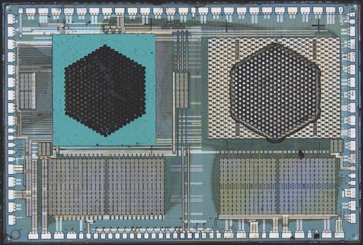
Artificial intelligence (AI) is driving an unprecedented surge in demand for compute and memory performance, driven by applications like ChatGPT based on large language models (LLMs). These sophisticated models have an insatiable appetite for computing power and fast memory access, resulting in an urgent and growing demand for much higher-density, low-power interconnects between Graphics Processing Units (GPUs) and high-bandwidth memory (HBM) modules. Today, HBM modules must be co-packaged with GPUs because the GPU-memory electrical interconnect is limited to just a few millimeters in length. Conventional optical interconnects based on VCSELs or Silicon Photonics (SiPh) promise to extend the interconnect reach. However, they are challenged by the power, bandwidth density, latency, and cost requirements. By contrast, Avicena's microLED-based LightBundle interconnects provide much lower power and latency, much higher bandwidth density, and can achieve very low costs.
About the Technology
Today's high-performance ICs use SerDes-based electrical interfaces to achieve adequate off-chip density. However, the power consumption and bandwidth density of these electrical links degrade quickly with length. Conventional optical communications technologies developed for networking applications have been impractical for inter-processor and processor-memory interconnects due to their low bandwidth density, high power consumption, and high cost. The typical need for external laser sources (ELS) with SiPh increases complexity and cost. By contrast the LightBundle interconnect architecture is based on arrays of innovative GaN microLEDs that leverage the microLED display ecosystem and can be integrated directly onto high performance CMOS ICs. Each microLED array is connected via a multi-core fiber cable to a matching array of CMOS-compatible PDs.
"We have previously demonstrated microLEDs transmitting at > 10 Gbps per lane and a test ASIC in a 130 nm CMOS process running 32 lanes at less than 1pJ/bit," says Bardia Pezeshki, founder and CEO of Avicena. "Now we are bringing up our first ASIC in a 16 nm finFET process with over 300 lanes and an aggregate bandwidth of over 1Tbps bi-directional at 4 Gbps per lane. The ASIC measures less than 12 mm² and contains the circuitry for the optical Tx and Rx arrays, as well as a high-speed parallel electrical interface and various DFT/DFM functions like BERT, loopbacks, and Open Eye Monitoring (OEM). All key ASIC functionality has been verified and we are currently working on yield improvements for manufacturing scalability."
In the future the modular nature of the LightBundle platform will enable interconnects with high-bandwidth density of multi-Tbps per mm² in advanced CMOS process nodes. The low power, high density, and low latency of LightBundle is well matched to chiplet interfaces like UCIe, OpenHBI, and BoW, and can also be used to enhance system architectures that are limited by the reach of existing compute interconnects like PCIe/CXL, and HBM/DDR/GDDR memory links.
Source:
Avicena
"As generative AI continues to evolve, the role of high bandwidth-density, low-power and low latency interconnects between xPUs and HBM modules cannot be overstated", says Chris Pfistner, VP Sales & Marketing of Avicena. "Avicena's innovative LightBundle interconnects have the potential to fundamentally change the way processors connect to each other and to memory because their inherent parallelism is well-matched to the internal wide and slow bus architecture within ICs. With a roadmap to multi-terabit per second capacity and sub-pJ/bit efficiency these interconnects are poised to enable the next era of AI innovation, paving the way for even more capable models and a wide range of AI applications that will shape the future."
Artificial intelligence (AI) is driving an unprecedented surge in demand for compute and memory performance, driven by applications like ChatGPT based on large language models (LLMs). These sophisticated models have an insatiable appetite for computing power and fast memory access, resulting in an urgent and growing demand for much higher-density, low-power interconnects between Graphics Processing Units (GPUs) and high-bandwidth memory (HBM) modules. Today, HBM modules must be co-packaged with GPUs because the GPU-memory electrical interconnect is limited to just a few millimeters in length. Conventional optical interconnects based on VCSELs or Silicon Photonics (SiPh) promise to extend the interconnect reach. However, they are challenged by the power, bandwidth density, latency, and cost requirements. By contrast, Avicena's microLED-based LightBundle interconnects provide much lower power and latency, much higher bandwidth density, and can achieve very low costs.
About the Technology
Today's high-performance ICs use SerDes-based electrical interfaces to achieve adequate off-chip density. However, the power consumption and bandwidth density of these electrical links degrade quickly with length. Conventional optical communications technologies developed for networking applications have been impractical for inter-processor and processor-memory interconnects due to their low bandwidth density, high power consumption, and high cost. The typical need for external laser sources (ELS) with SiPh increases complexity and cost. By contrast the LightBundle interconnect architecture is based on arrays of innovative GaN microLEDs that leverage the microLED display ecosystem and can be integrated directly onto high performance CMOS ICs. Each microLED array is connected via a multi-core fiber cable to a matching array of CMOS-compatible PDs.
"We have previously demonstrated microLEDs transmitting at > 10 Gbps per lane and a test ASIC in a 130 nm CMOS process running 32 lanes at less than 1pJ/bit," says Bardia Pezeshki, founder and CEO of Avicena. "Now we are bringing up our first ASIC in a 16 nm finFET process with over 300 lanes and an aggregate bandwidth of over 1Tbps bi-directional at 4 Gbps per lane. The ASIC measures less than 12 mm² and contains the circuitry for the optical Tx and Rx arrays, as well as a high-speed parallel electrical interface and various DFT/DFM functions like BERT, loopbacks, and Open Eye Monitoring (OEM). All key ASIC functionality has been verified and we are currently working on yield improvements for manufacturing scalability."
In the future the modular nature of the LightBundle platform will enable interconnects with high-bandwidth density of multi-Tbps per mm² in advanced CMOS process nodes. The low power, high density, and low latency of LightBundle is well matched to chiplet interfaces like UCIe, OpenHBI, and BoW, and can also be used to enhance system architectures that are limited by the reach of existing compute interconnects like PCIe/CXL, and HBM/DDR/GDDR memory links.
2 Comments on Avicena Demonstrates First microLED Based Transceiver IC in 16 nm finFET CMOS for Chip-to-Chip Communications
"parallel electrical interface", I guess this solution may link GPU or xPU directly by its 300 or more lanes. Otherwise, it needs electrical mux/demux which would be power-consuming.
If 300 or more lanes parallely, then there should be an interface protocol between GPU/xPU and this "parallel electrical interface" with a fixed lane number. Let's say 256 or 512 lanes for example. If using a normal micro LED, the bandwidth would be around 2GHz, which means 4~5Gbps by NRZ. If a RCLED, maybe 10Gbps per lane. 10Gbps * 512 = 5Tbps may be a maximum limitation. Of course, the current topic is about 1Tbps.
I am not sure about the "ASIC in 16 nm finFET CMOS". Is it possible to make this ASIC in 90nm process?