News Posts matching #2 nm

Return to Keyword Browsing

TSMC Said to Start Construction of 1.4 nm Fab in 2026

According to Taiwanese media, TSMC will start production of its first 1.4 nm fab in 2026, with chip production in the fab said to start sometime in 2027 or 2028. The new fab will be located in Longtan Science Park outside of Hsinchu in Taiwan, where many of TSMC's current fabs are located. TSMC is currently constructing a 2 nm and below node R&D facility at a nearby plot of land to where the new fab is expected to be built. This facility is expected to be finished in 2025 and TSMC has been allocated a total area of just over 158 hectares of land for future expansion in the area.

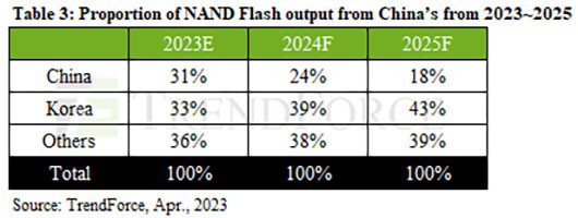
In related news, TSMC is expected to be charging US$25,000 per 2 nm GAA wafer, which is an increase of about a fifth compared to its 3 nm wafers which are going for around US$20,000. This is largely due to the nodes being fully booked and TSMC being able to charge a premium for its cutting edge nodes. TSMC is also expanding in CoWoS packaging facilities due to increased demand from both AMD and NVIDIA for AI related products. Currently TSMC is said to be able to output 12,000 CoWoS wafers per month and this is twice as much as last year, yet TSMC is unable to meet demand from its customers.

Samsung Electronics Unveils Foundry Vision in the AI Era

Samsung Electronics, a world leader in advanced semiconductor technology, today announced its latest foundry technology innovations and business strategy at the 7th annual Samsung Foundry Forum (SFF) 2023. Under the theme "Innovation Beyond Boundaries," this year's forum delved into Samsung Foundry's mission to address customer needs in the artificial intelligence (AI) era through advanced semiconductor technology.

Over 700 guests, from customers and partners of Samsung Foundry, attended this year's event, of which 38 companies hosted their own booths to share the latest technology trends in the foundry industry.

Top 10 Foundries Report Nearly 20% QoQ Revenue Decline in 1Q23, Continued Slide Expected in Q2

TrendForce reports that the global top 10 foundries witnessed a significant 18.6% QoQ decline in revenue during the first quarter of 2023. This decline—amounting to approximately US$27.3 billion—can be attributed to sustained weak end-market demand and the compounded effects of the off-peak season. The rankings also underwent notable changes, with GlobalFoundries surpassing UMC to secure the third position, and Tower Semiconductor surpassing PSMC and VIS to claim the seventh spot.

Declining capacity utilization rate and shipment volume contribute to widened revenue decline
The revenue decline in Q1 was primarily influenced by declining capacity utilization rates and shipment volume across the top 10 foundries. For instance, TSMC generated US$16.74 billion in revenue—marking a 16.2% QoQ drop in revenue. Weakened demand for mainstream applications such as laptops and smartphones led to a significant decline in the utilization rates and revenue of the 7/6 nm and 5/4 nm processes, falling over 20% and 17%, respectively. While the second quarter may see temporary relief coming from rush orders, the persistently low capacity utilization rate indicates that revenue is likely to continue declining, albeit at a slower pace compared to Q1.

Samsung Electronics Announces First Quarter 2023 Results, Profits Lowest in 14 Years

Samsung Electronics today reported financial results for the first quarter ended March 31, 2023. The Company posted KRW 63.75 trillion in consolidated revenue, a 10% decline from the previous quarter, as overall consumer spending slowed amid the uncertain global macroeconomic environment. Operating profit was KRW 0.64 trillion as the DS (Device Solutions) Division faced decreased demand, while profit in the DX (Device eXperience) Division increased.

The DS Division's profit declined from the previous quarter due to weak demand in the Memory Business, a decline in utilization rates in the Foundry Business and continued weak demand and inventory adjustments from customers. Samsung Display Corporation (SDC) saw earnings in the mobile panel business decline quarter-on-quarter amid a market contraction, while the large panel business slightly narrowed its losses. The DX Division's results improved on the back of strong sales of the premium Galaxy S23 series as well as an enhanced sales mix focusing on premium TVs.

TSMC Showcases New Technology Developments at 2023 Technology Symposium

TSMC today showcased its latest technology developments at its 2023 North America Technology Symposium, including progress in 2 nm technology and new members of its industry-leading 3 nm technology family, offering a range of processes tuned to meet diverse customer demands. These include N3P, an enhanced 3 nm process for better power, performance and density, N3X, a process tailored for high performance computing (HPC) applications, and N3AE, enabling early start of automotive applications on the most advanced silicon technology.

With more than 1,600 customers and partners registered to attend, the North America Technology Symposium in Santa Clara, California is the first of the TSMC's Technology Symposiums around the world in the coming months. The North America symposium also features an Innovation Zone spotlighting the exciting technologies of 18 emerging start-up customers.

Rapidus to Start Production of 2 nm Fab in Chitose, Gets Cash Injection from Japanese Government

Future Japanese chipmaker Rapidus has announced that their first fab will be located in Chitose, Hokkaido, located in northern Japan. The planned 2 nm fab will be one of the most advanced fabs in the world once it's ready and construction is said to be starting in September, thanks to approval by the related Japanese government agencies. So far, the Japanese government has approved 330 billion yen for Rapidus, with the most recent investment being 260 billion yen or the equivalent of US$1.94 billion.

However, the total investment into the 2 nm fab is expected to end up somewhere around 5 trillion yen (~US$37.5 billion) in total investments before the fab is ready for mass production. Rapidus is collaborating with IBM and has already sent a group of researchers to its Albany Nanotech facility in upstate New York, which is one of the world's most advanced semiconductor research facilities. At the same time, Japan is working on building a local talent pool of researchers and semiconductor plant workers, by spearheading specialised training for select university students from Japan's top universities. Time will tell if this gamble pays off for Japan, as it's going to be a huge investment before the new fab stands ready in early 2025.

Strict Restrictions Imposed by US CHIPS Act Will Lower Willingness of Multinational Suppliers to Invest

TrendForce reports that the US Department of Commerce recently released details regarding its CHIPS and Science Act, which stipulates that beneficiaries of the act will be restricted in their investment activities—for more advanced and mature processes—in China, North Korea, Iran, and Russia for the next ten years. The scope of restrictions in this updated legislation will be far more extensive than the previous export ban, further reducing the willingness of multinational semiconductor companies to invest in China for the next decade.

CHIPS Act will mainly impact TSMC; and as the decoupling of the supply chain continues, VIS and PSMC capture orders rerouted from Chinese foundries
In recent years, the US has banned semiconductor exports and passed the CHIPS Act, all to ensure supply chains decoupling from China. Initially, bans on exports were primarily focused on non-planar transistor architecture (16/14 nm and more advanced processes). However, Japan and the Netherlands have also announced that they intend to join the sanctions, which means key DUV immersion systems, used for producing both sub-16 nm and 40/28 nm mature processes, are likely to be included within the scope of the ban as well. These developments, in conjunction with the CHIPS Act, mean that the expansion of both Chinese foundries and multinational foundries in China will be suppressed to varying degrees—regardless of whether they are advanced or mature processes.

AMD Zen 5 "Nirvana" and Zen 6 "Morpheus" Core Codenames Leaked, Confirm Foundry Nodes

An AMD engineer inadvertently leaked the core codenames of the company's upcoming "Zen 5" and "Zen 6" microarchitectures. It's important to understand here what has been leaked. "Zen 5" and "Zen 6" are microarchitecture names, just like the current "Zen 4" and past "Zen 3" or older. AMD uses codenames for the CCD (CPU complex dies) based on these microarchitectures, which it shares between Ryzen client and EPYC enterprise processors. For example, the CCD codename for "Zen 3" is "Brekenridge," and for "Zen 4" it is "Durango." AMD also uses codenames for the CPU cores themselves. "Zen 3" CPU cores are codenamed "Cerebrus," and "Zen 4" CPU cores "Persphone." And now, the leak:

The CCD based on the upcoming "Zen 5" microarchitecture is codenamed "Eldora," and the "Zen 5" CPU core itself is codenamed "Nirvana." There's no codename for the CCD based on "Zen 6," but its CPU cores are codenamed "Morpheus." The "Zen 5" microarchitecture will be based on the 3 nm EUV foundry node; while "Zen 6" will be 2 nm EUV. The engineer in the screenshot is contributing to the power-management technology behind "Zen 5" and "Zen 6," and states that their work on "Zen 5" spanned January-December of 2022, which means the development phase of the next "Zen" architecture is probably complete, and the architecture is undergoing testing and refinement. It's also claimed that work on at least the power-management aspect of "Zen 6" has started from January 2023.

Intel 20A and 18A Foundry Nodes Complete Development Phase, On Track for 2024 Manufacturing

Intel Foundry Services, the in-house semiconductor foundry of Intel, announced that its 2 nm-class Intel 20A and 1.8 nm-class Intel 18A foundry nodes have completed development, and are on course for mass-producing chips on their roadmap dates. Chips are expected to begin mass-production on the Intel 20A node in the first half of 2024, while those on the Intel 18A node are expected to begin in the second half of 2024. The completion of the development phase means that Intel has finalized the specifications and performance/power targets of the nodes, the tools and software required to make the chips, and can now begin ordering them to build the nodes. Intel has been testing these nodes through 2022, and with the specs being finalized, chip-designers can accordingly wrap up development of their products to align with what these nodes have to offer.

Intel 20A (or 20-angstrom, or 2 nm) node introduces gates-all-around (GAA) RibbonFET transistors with PowerVIAs (an interconnect innovation that contributes to transistor densities). The Intel 20A node is claimed to offer a 15% performance/Watt gain over its predecessor, the Intel 3 node (FinFET EUV, 3 nm-class), which by itself offers an 18% performance/Watt gain over Intel 4 (20% perf/Watt gain over the current Intel 7 node), the node that is entering mass-production very soon. The Intel 18A node is a further refinement of Intel 20A, and introduces a design improvement to the RibbonFET that increases transistor density at scale, and a claimed 10% performance/Watt improvement over Intel 20A.

Samsung Electronics Announces Fourth Quarter and FY 2022 Results, Profits at an 8-year Low

Samsung Electronics today reported financial results for the fourth quarter and the fiscal year 2022. The Company posted KRW 70.46 trillion in consolidated revenue and KRW 4.31 trillion in operating profit in the quarter ended December 31, 2022. For the full year, it reported 302.23 trillion in annual revenue, a record high and KRW 43.38 trillion in operating profit.

The business environment deteriorated significantly in the fourth quarter due to weak demand amid a global economic slowdown. Earnings at the Memory Business decreased sharply as prices fell and customers continued to adjust inventory. The System LSI Business also saw a decline in earnings as sales of key products were weighed down by inventory adjustments in the industry. The Foundry Business posted a new record for quarterly revenue while profit increased year-on-year on the back of advanced node capacity expansion as well as customer base and application area diversification.

TSMC Holds 3nm Volume Production and Capacity Expansion Ceremony, Marking a Key Milestone for Advanced Manufacturing

TSMC today held a 3 nanometer (3 nm) Volume Production and Capacity Expansion Ceremony at its Fab 18 new construction site in the Southern Taiwan Science Park (STSP), bringing together suppliers, construction partners, central and local government, the Taiwan Semiconductor Industry Association, and members of academia to witness an important milestone in the Company's advanced manufacturing.

TSMC has laid a strong foundation for 3 nm technology and capacity expansion, with Fab 18 located in the STSP serving as the Company's GIGAFAB facility producing 5 nm and 3 nm process technology. Today, TSMC announced that 3 nm technology has successfully entered volume production with good yields, and held a topping ceremony for its Fab 18 Phase 8 facility. TSMC estimates that 3 nm technology will create end products with a market value of US$1.5 trillion within five years of volume production.

Apple and NVIDIA First Customers of TSMC's Arizona Fab

Apple and NVIDIA will be among the first customers of TSMC's swanky new $12 billion semiconductor fab in Arizona, USA. Apple will be the first major player to kick off mass-production in the fab, and will be closely followed by NVIDIA. Both companies plan to produce some of their inventory in Arizona, and ramp proportionately up as the fab grows in capacity.

The plan with TSMC's Arizona fab was to originally make 5 nm and 4 nm EUV chips, with an output of 20,000 wafers a month, but the company now expects to deploy a more advanced node to keep up with what will be considered cutting-edge when the fab goes live (think 2 nm-class); and also double the output to 40,000 wafers a month. The capacity should ensure Apple and NVIDIA make their most cutting-edge chips on the node (away from Asia), so there could be tighter export controls, and build supply-chain resilience in the face of security problems arising in the Taiwan straits.

Intel's Next-Gen Desktop Platform Intros Socket LGA1851, "Meteor Lake-S" to Feature 6P+16E Core Counts

Keeping up with the cadence of two generations of desktop processors per socket, Intel will turn the page of the current LGA1700, with the introduction of the new Socket LGA1851. The processor package will likely have the same dimensions as LGA1700, and the two sockets may share cooler compatibility. The first processor microarchitecture to debut on LGA1851 will be the 14th Gen Core "Meteor Lake-S." These chips will feature a generationally lower CPU core-count compared to "Raptor Lake," but significantly bump the IPC on both the P-cores and E-cores.

"Raptor Lake" is Intel's final monolithic silicon client processor before the company pivots to chiplets built on various foundry nodes, as part of its IDM 2.0 strategy. The client-desktop version of "Meteor Lake," dubbed "Meteor Lake-S," will have a maximum CPU core configuration of 6P+16E (that's 6 performance cores with 16 efficiency cores). The chip has 6 "Redwood Cove" P-cores, and 16 "Crestmont" E-cores. Both of these are expected to receive IPC uplifts, such that the processor will end up faster (and hopefully more efficient) than the top "Raptor Lake-S" part. Particularly, it should be able to overcome the deficit of 2 P-cores.

Samsung Electronics Unveils Plans for 1.4 nm Process Technology

Samsung Electronics, a world leader in advanced semiconductor technology, announced today a strengthened business strategy for its Foundry Business with the introduction of cutting-edge technologies at its annual Samsung Foundry Forum event. With significant market growth in high-performance computing (HPC), artificial intelligence (AI), 5/6G connectivity and automotive applications, demand for advanced semiconductors has increased dramatically, making innovation in semiconductor process technology critical to the business success of foundry customers. To that end, Samsung highlighted its commitment to bringing its most advanced process technology, 1.4-nanometer (nm), for mass production in 2027.

During the event, Samsung also outlined steps its Foundry Business is taking in order to meet customers' needs, including: foundry process technology innovation, process technology optimization for each specific applications, stable production capabilities, and customized services for customers. "The technology development goal down to 1.4 nm and foundry platforms specialized for each application, together with stable supply through consistent investment are all part of Samsung's strategies to secure customers' trust and support their success," said Dr. Si-young Choi, president and head of Foundry Business at Samsung Electronics. "Realizing every customer's innovations with our partners has been at the core of our foundry service."

AMD's CEO Lisa Su Planning Trip to Taiwan, Said to be Visiting TSMC to Secure Future Wafer Allocation

Based on a report by Tom's Hardware, AMD's CEO Lisa Su is planning a trip to Taiwan in the next couple of months. It is said that she is planning to meet with multiple partners in Taiwan, such as ASUS, Acer and maybe more importantly, ASMedia, which will be the sole maker of chipsets for AMD, once the X570 chipset is discontinued. AMD is apparently also seeing various less well known partners that deliver parts for its CPUs, such as Nan Ya PCB, Unimicron Technologies and Kinsus Interconnects.

However, it appears that the main reason for Lisa Su herself to visit Taiwan will be to meet with TSMC, to discuss future collaboration with CC Wei, TSMC's chief executive. This is so AMD can secure enough wafer allocation on future nodes, such as its 3 nm and 2 nm class nodes. The move to these nodes is obviously not happening in the near future for AMD, but considering that TSMC is currently the leading foundry and is operating at capacity, it makes sense to get in early, as the competition is stiff when it comes to getting wafer allocation on cutting edge nodes. It's unclear which exact 3 nm class node AMD will be aiming for, but it might be the N3P node, which is said to kick off production sometime next year. Lisa Su is also said to have meetings with TSMC, SPIL and Ase Technology when it comes to advanced packaging for AMD's products. This includes technologies such as chip-on-wafer-on-substrate (CoWoS) and fan-out embedded bridge (FO-EB), with AMD already being expected to use some of these technologies in its upcoming Navi 3x GPUs.

US Institutes GAA-FET Technology EDA Software Ban on China, Stalling sub-3nm Nodes

The US Government has instituted a ban on supply of GAA-FET EDA software to China (the Chinese government and companies in China). Humans can no longer design every single circuit on chips with tens of billions of transistors, and so EDA (electronics design automation) software is used to micromanage design based broadly on what chip architects want. Synopsys, Cadence, and Siemens are major EDA software suppliers. Intel is rumored to use an in-house EDA software that it doesn't sell, although this could change with the company roping in third-party foundries, such as TSMC, for cutting-edge logic chips (which will need the software to make sense of Intel's designs).

GAA or "gates-all-around" technology is vital to building transistors in the 3 nm and 2 nm silicon fabrication nodes. Samsung is already using GAA for its 3 nm node, while TSMC intends to use it with its 2N (2 nm) node. Intel is expected to use it with its Intel 20A (20 angstrom, or 2 nanometers) node. Both Intel and TSMC will debut nodes powered by GAAFETs for mass-production in 2024. The US Government has already banned the sales of EUV lithography machines to China, as well as machines fabricating 3D NAND flash chips with greater than 128 layers or 14 nm. In the past, technology embargoes have totally stopped China from copying or reverse-engineering western tech, or luring Taiwanese engineers armed with industry secrets away on the promise of wealth and a comfortable life in the Mainland.

Japan and the US Joins Forces to Produce 2 nm Chips in Japan by 2025

Based on a report by the Nikkei, Japan and the US have joined forces to speed up the development of semiconductor production at 2 nm nodes in Japan by 2025. It's not exactly clear how this is going to happen, but the two nations are said to have signed a bilateral chip technology partnership. The heavy lifting is said to be done by private companies from both nations, but in terms of research and actual chip production. Part of the reason for the move, is that Japan wants to be able to manufacture cutting edge ICs domestically for next-generation chips.

The research is said to be kicking off as soon as this summer, although no decisions have been made with regards to the manufacturing structure, with the Nikkei suggesting two alternatives, based on information from the Japanese Ministry of Economy. There will either be a joint partnership between Japanese and US businesses, or it could be a wholly Japanese owned setup. It appears that one major reason for this project is the production of ICs for the Japanese defence industry, as advanced electronics are needed in a lot of related products, ranging from fighter jets and missiles, to radar systems and communication systems. However, the article also suggests that the 2 nm node is suitable for everything from components for quantum computers to smartphones. Japan already makes advanced silicon wafers and many other parts and components used in semiconductor manufacturing, but the nation has fallen behind in the actual manufacturing of leading edge semiconductors over the past few years.

Apple, Intel to Become Alpha Customers for TSMC's 2 nm Manufacturing Node

Industry reports and sources in the financial community have placed Apple and Intel as the two premier customers for TSMC's upcoming N2 node. N2, which is expected to enter volume production by the end of 2025, will be TSMC's first manufacturing process making use of GAAFET (Gate-All-Around Field-Effect Transistor) design. If there are no significant market upheavals or unexpected snags in technology transition, TSMC will be late to the GAAFET party, following Samsung's 3GAE node in 2023 and Intel's first Angstrom-era process, Intel 20A, in 2024.

While Apple's uptake on TSMC's latest manufacturing technology is practically a given at this point, the fact that Intel too is taking up TSMC's N2 node showcases the company's evolved business tactics after the introduction of its IDM 2.0 strategy (IDM standing for Integrated Device Manufacturer, meaning Intel too will fabricate chips according to clients' specs). While pre-Pat Gelsinger was seemingly scared of touching any other foundries' products - mostly from the fact that Intel does have its own significant manufacturing capabilities and R&D, after all - the new Intel is clearly more at peace with driving its competitor's revenues.

TSMC to Start 2 nm Production by 2025, 3 nm by the End of 2022

Responding to investor questions in TSMC's first quarter earnings call for 2022, CEO C. C. Wei reiterated that the company's upcoming manufacturing processes are generally moving smoothly throughout development. Even as TSMC announced historic revenues on the back of increased pricing throughout the semiconductor industry, the company is showing no signs of slowing down on its development. When further asked regarding the company's ability to navigate the world's troubled, inflation-ridden waters, Wei added that TSMC's strategic positioning as the leading semiconductor foundry makes it resilient to market and demand fluctuations.

TSMC's roadmap has seen multiple accelerations of late, which have placed 3 nm tape-out to occur before the end of the year. Perhaps more significantly, the company's next-generation 2 nm manufacturing process, which will make use of GAA (Gate All Around) transistor designs for greater design efficiency and density, are still on track for a 2025 volume production following an expected 2024 tape-out.

Samsung Foundry Looks to Legacy Nodes for Expansion

While there's a lot of talk about cutting edge nodes, Samsung Foundries are looking at alternative options to find new business and are said to be eyeing legacy nodes for future expansions. At the same time, Samsung is looking at setting up its own chip testing and packaging factory, to be able to better serve customers who are looking for a full-service partner. It's not clear which legacy nodes Samsung are eyeing, but the story by Business Korea states that at least some of it will focus on CMOS imaging sensors, since there is apparently a shortage of those too.

Samsung is said to have plans for no less than 300 new customers by 2026 for its foundry business, across all nodes. However, this doesn't mean Samsung will stop developing new, cutting edge nodes, as Samsung is still planning to kick off volume production on its 3 nm node in the first half of this year, with 2 nm said to start volume production in 2025. After its dealings with Nvidia and Qualcomm that haven't been what you'd call successful, the question is who will be willing to partner with Samsung Foundry on its cutting edge nodes in the future.

Report: Intel to Become One of the Three Largest TSMC Clients in 2023

Intel and TSMC are positioning themselves as two competing foundries for a significant period. However, as the difficulties in semiconductor manufacturing rise, the collaboration of the two seems inevitable. Not because Intel is eyeing TSMC's clients, but because of the race to produce the most minor and best possible semiconductor node. We already know that Intel plans to use some of TSMC's nodes for its Ponte Vecchio accelerator that contains 47 tiles. However, we didn't realize just how big the contract between the two companies was. According to the latest report from DigiTimes, Intel is supposed to become one of the top three clients at TSMC.

As the report notes, the collaboration should extend to at least TSMC's 2 nm node, expected in 2025. After that, the state of semiconductors is unknown. Intel has a solid chance to be in the top three customers in 2023 and become one of the primary sources of profit for the Taiwanese giant. We are excited to see how this prediction plays out and hope to hear more from both in the future.

Samsung Foundry Announces GAA Ready, 3nm in 2022, 2nm in 2025, Other Speciality Nodes

Samsung Electronics, a world leader in advanced semiconductor technology, today unveiled plans for continuous process technology migration to 3- and 2-nanometer (nm) based on the company's Gate-All-Around (GAA) transistor structure at its 5th annual Samsung Foundry Forum (SFF) 2021. With a theme of "Adding One More Dimension," the multi-day virtual event is expected to draw over 2,000 global customers and partners. At this year's event, Samsung will share its vision to bolster its leadership in the rapidly evolving foundry market by taking each respective part of foundry business to the next level: process technology, manufacturing operations, and foundry services.

"We will increase our overall production capacity and lead the most advanced technologies while taking silicon scaling a step further and continuing technological innovation by application," said Dr. Siyoung Choi, President and Head of Foundry Business at Samsung Electronics. "Amid further digitalization prompted by the COVID-19 pandemic, our customers and partners will discover the limitless potential of silicon implementation for delivering the right technology at the right time."

Fabricating the Fabs: ASML Vision Document Predicts 300 Billion-Transistor Logic by 2030

"Moore's Law is alive and well," says ASML, in its vision document addressing investors. The company manufactures the machines that perform the actual task of silicon lithography—turning silicon discs into wafers of logic or storage chips. It highlighted the various technologies making progress, which will help its semiconductor-fabrication customers, such as TSMC and their hundreds of clients, sustain Moore's Law all the way through this decade. The company predicts SoCs with as many as 300 billion transistors by 2030. To achieve this, the company is innovating in two distinct directions—at the chip-level, to increase transistor density per chip to over 50 billion transistors; and at the system level, through packaging technology innovations, to reach that ultimate transistor count.

According to ASML's roadmap, at the turn of the decade, its technology enables 5 nm-class in production, and is at the cusp of a major breakthrough, nanosheet-FETs. which pave the way for 3 nm and 2 nm nodes, backed by EUV lithography. The journey from 2 nm to 1.5 nm will require another breakthrough, forked-nanosheets, and from 1.5 nm to 1 nm yet another breakthrough, CFET. Sub-1 nm fabrication will be possible toward the turn of this decade, thanks to 2D atomic channel technology, which is how chip-designers will be able to cram over 50 billion transistors per chip, and build MCM systems with over 300 billion transistors. The presentation predicts that besides 3D packaging, stacked silicon will also play a role, with multiple stacked logic layers, heterogenous chips with logic, storage, and I/O layers, stacked DRAM (up from single-digit layers to double-digits; and for NAND flash to grow from the current 176-layer, to nearly 500-layer by 2030.

IBM Unveils On-Chip Accelerated Artificial Intelligence Processor

At the annual Hot Chips conference, IBM (NYSE: IBM) today unveiled details of the upcoming new IBM Telum Processor, designed to bring deep learning inference to enterprise workloads to help address fraud in real-time. Telum is IBM's first processor that contains on-chip acceleration for AI inferencing while a transaction is taking place. Three years in development, the breakthrough of this new on-chip hardware acceleration is designed to help customers achieve business insights at scale across banking, finance, trading, insurance applications and customer interactions. A Telum-based system is planned for the first half of 2022.

Today, businesses typically apply detection techniques to catch fraud after it occurs, a process that can be time consuming and compute-intensive due to the limitations of today's technology, particularly when fraud analysis and detection is conducted far away from mission critical transactions and data. Due to latency requirements, complex fraud detection often cannot be completed in real-time - meaning a bad actor could have already successfully purchased goods with a stolen credit card before the retailer is aware fraud has taken place.

Intel Rebadges 10nm Enhanced SuperFin Node as "Intel 7," Invents Other Creative Node Names

Intel, in a move comparable to its competitors' Performance Rating system from the 1990s, has invented a new naming scheme for its in-house foundry nodes to claim technological parity with contemporaries such as TSMC and Samsung, that are well into the sub-10 nm class. Back in the i586 era, when Intel's competitors such as AMD and Cyrix, couldn't keep up with its clock-speeds yet found their chips to be somewhat competitive, they invented the PR (processor rating) system, with a logical number attempting to denote parity with an Intel processor's clock-speed. For example, a PR400 processor rating meant that the chip rivaled a Pentium II 400 MHz (which it mostly didn't). The last that the PR system made sense was with the final generation of single-core performance chips, Pentium 4 and Athlon XP, beyond which, the introduction of multi-core obfuscated the PR system. A Phenom X4 9600 processor didn't mean performance on par with a rival Intel chip running at an impossible 9.60 GHz.

Intel's new foundry naming system sees its 10 nm Enhanced SuperFin node re-badge as "Intel 7." The company currently builds 11th Gen Core "Tiger Lake" processors on the 10 nm SuperFin node, and is expected to build its upcoming 12th Gen Core "Alder Lake" chips on its refinement, the 10 nm Enhanced SuperFin, which will now be referred to as "Intel 7." The company is careful to avoid using the nanometer unit next to the number, instead signaling the consumer that the node somehow offers transistor density and power characteristics comparable to a 7 nm node. Intel 7 offers a 10-15 percent performance/Watt gain over 10 nm SuperFin, and is already in volume production, with a debut within 2021 with "Alder Lake."
Return to Keyword Browsing
May 21st, 2024 16:42 EDT change timezone

New Forum Posts

Popular Reviews

Controversial News Posts