News Posts matching #2022

Return to Keyword Browsing

Silicon Motion: PCIe 5.0 SSD Controller to Arrive Next Year

With the debut of PCIe 4.0 standard, SSD manufacturers have started launching a new generation of storage devices, with unseen speeds before. Today's PCIe 4.0 SSDs can reach up to 8.0 GB/s reads and writes, all thanks to the bandwidth-heavy PCIe protocol. However, enterprise workloads are always requiring more and more bandwidth to satisfy their needs. Data is being moved in immense quantities and faster hardware is always welcome. The previous PCIe 4.0 standard is about to kneel to its successor - PCIe 5.0 protocol. Having double the amount of bandwidth, the new standard is set to bring unseen speeds.

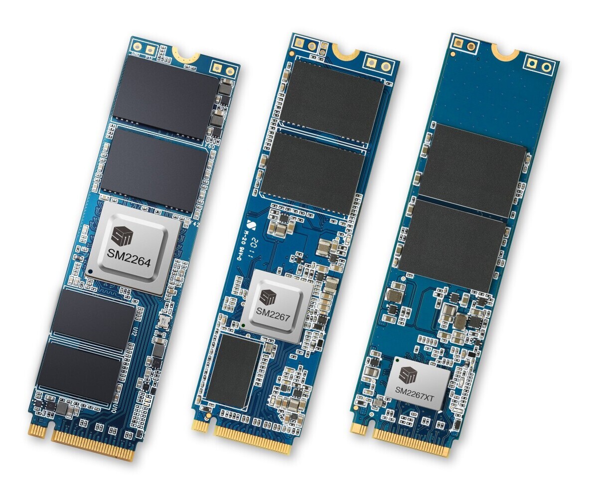
The PCIe 5.0 protocol offers 32 GT/s per lane, making up to 64 GB/s in the full x16 implementation. However, when it comes to SSDs, as they use x4 lanes, it will increase the maximum speed to 16 GB/s, doubling the previous bandwidth. Silicon Motion, the maker of NAND flash controllers, has announced that the company is going to debut a PCIe 5.0 controller next year. "We are excited about enterprise-grade PCIe Gen5 controller, which we will have taped out early next year and sample in the second half of 2022", said Wallace Kuo, chief executive of Silicon Motion, during a conference call. Launching just in time to pair with Intel's Sapphire Rapids Xeon processors that support the PCIe 5.0 protocol, Silicon Motion is probably expecting to grab its market share there.

AMD is Allegedly Preparing Navi 31 GPU with Dual 80 CU Chiplet Design

AMD is about to enter the world of chiplets with its upcoming GPUs, just like it has been doing so with the Zen generation of processors. Having launched a Radeon RX 6000 series lineup based on Navi 21 and Navi 22, the company is seemingly not stopping there. To remain competitive, it needs to be in the constant process of innovation and development, which is reportedly true once again. According to the current rumors, AMD is working on an RDNA 3 GPU design based on chiplets. The chiplet design is supposed to feature two 80 Compute Unit (CU) dies, just like the ones found inside the Radeon RX 6900 XT graphics card.

Having two 80 CU dies would bring the total core number to exactly 10240 cores (two times 5120 cores on Navi 21 die). Combined with the RDNA 3 architecture, which brings better perf-per-watt compared to the last generation uArch, Navi 31 GPU is going to be a compute monster. It isn't exactly clear whatever we are supposed to get this graphics card, however, it may be coming at the end of this year or the beginning of the following year 2022.

TrendForce: TSMC to Mass-Produce Select Intel Products, CPUs Starting 2021

According to a market analysis from TrendForce, Intel's manufacturing efforts with TSMC will go way beyond a potential TSMC technology licensing for that company's manufacturing technology to be employed in Intel's own fabs. The market research firm says that Intel will instead procure wafers directly from TSMC, starting on 2H2021, in the order of 20-25% of total production for some of its non-CPU products. But the manufacturing deal is said to go beyond that, with TSMC picking up orders for Intel's Core i3 CPUs in the company's 5 nm manufacturing node - one that Intel will take years to scale down to on its own manufacturing capabilities.

According to TrendForce, that effort will scale upwards with TSMC manufacturing certain allotments of Intel's midrange and high-end CPUs using the semiconductor manufacturer's 3 nm technology in 2022. TrendForce believes that increased outsourcing of Intel's product lines will allow the company to not only continue its existence as a major IDM, but also maintain and prioritize in-house production lines for chips with high margins, while more effectively spending CAPEX on advanced R&D due to savings on fabrication technology scaling - fewer in-house chips means lower needs for investment in capacity increases, which would allow the company to sink the savings into further R&D. The move would also allow Intel to close the gap with rival AMD's manufacturing advantages in a more critical, timely manner.

NVIDIA to Introduce an Architecture Named After Ada Lovelace, Hopper Delayed?

NVIDIA has launched its GeForce RTX 3000 series of graphics cards based on the Ampere architecture three months ago. However, we are already getting information about the next-generation that the company plans to introduce. In the past, the rumors made us believe that the architecture coming after Ampere is allegedly being called Hopper. Hopper architecture is supposed to bring multi-chip packaging technology and be introduced after Ampere. However, thanks to @kopite7kimi on Twitter, a reliable source of information, we have data that NVIDIA is reportedly working on a monolithic GPU architecture that the company internally refers to as "ADxxx" for its codenames.

The new monolithically-designed Lovelace architecture is going make a debut on the 5 nm semiconductor manufacturing process, a whole year earlier than Hopper. It is unknown which foundry will manufacture the GPUs, however, both of NVIDIA's partners, TSMC and Samsung, are capable of manufacturing it. The Hopper is expected to arrive sometime in 2023-2024 and utilize the MCM technology, while the Lovelace architecture will appear in 2021-2022. We are not sure if the Hopper architecture will be exclusive to data centers or extend to the gaming segment as well. The Ada Lovelace architecture is supposedly going to be a gaming GPU family. Ada Lovelace, a British mathematician, has appeared on NVIDIA's 2018 GTC t-shirt known as "Company of Heroes", so NVIDIA may have already been using the ADxxx codenames internally for a long time now.

NAND Flash Revenue for 3Q20 up by Only 0.3% QoQ Owing to Weak Server Sales, Says TrendForce

Total NAND Flash revenue reached US$14.5 billion in 3Q20, a 0.3% increase QoQ, while total NAND Flash bit shipment rose by 9% QoQ, but the ASP fell by 9% QoQ, according to TrendForce's latest investigations. The market situation in 3Q20 can be attributed to the rising demand from the consumer electronics end as well as the recovering smartphone demand before the year-end peak sales season. Notably, in the PC market, the rise of distance education contributed to the growing number and scale of Chromebook tenders, but the increase in the demand for Chromebook devices has not led to a significant increase in NAND Flash consumption because storage capacity is rather limited for this kind of notebook computer. Moreover, clients in the server and data center segments had aggressively stocked up on components and server barebones during 2Q20 due to worries about the impact of the pandemic on the supply chain. Hence, their inventories reached a fairly high level by 3Q20. Clients are now under pressure to control and reduce their inventories during this second half of the year. With them scaling back procurement, the overall NAND Flash demand has also weakened, leading to a downward turn in the contract prices of most NAND Flash products.

TSMC Completes Its Latest 3 nm Factory, Mass Production in 2022

They say that it is hard to keep up with Moore's Law, however, for the folks over at Taiwan Semiconductor Manufacturing Company (TSMC), that doesn't seem to represent any kind of a problem. Today, to confirm that TSMC is one of the last warriors for the life of Moore's Law, we have information that the company has completed building its manufacturing facility for the next-generation 3 nm semiconductor node. Located in Southern Taiwan Science Park near Tainan, TSMC is expecting to start high-volume manufacturing of the 3 nm node in that Fab in the second half of 2022. As always, one of the first customers expected is Apple.

Estimated to cost an amazing 19.5 billion US Dollars, the Fab is expected to have an output of 55,000 300 mm (12-inch) wafers per month. Given that the regular facilities of TSMC exceed the capacity of over 100K wafers per month, this new facility is expected to increase the capacity over time and possibly reach the 100K level. The new 3 nm node is going to use the FinFET technology and will deliver a 15% performance gain over the previous 5 nm node, with 30% decreased power use and up to 70% density increase. Of course, all of those factors will depend on a specific design.

TSMC Partners With Google and AMD to Push 3D Silicon

Silicon manufacturing is starting to get harder and harder every day, with new challenges appearing daily. It requires massive investment and massive knowledge to keep a silicon manufacturing company afloat. No company can survive that alone, so some collaborations are emerging. Today, thanks to the sources of Nikkei Asia, we have information that Taiwanese Semiconductor Manufacturing Company (TSMC) is collaborating with Google to push the production of 3D chip manufacturing process, that is said to overcome some of the silicon manufacturing difficulties. The sources also say that AMD is involved in the process as well, making Google and AMD the first customers of the advanced 3D chip design. The two companies are preparing designs for the new way of creating silicon and will help TSMC test and certify the process.

TSMC will deploy the 3D silicon manufacturing technology at its chip packaging plant in Miaoli, which is supposed to do mass production in 2022. With Google and AMD being the first customers of new 3D technology, it is exciting to see what new products will look like and how they will perform. The 3D approach is said to bring huge computing power increase, however, it is a waiting game now to see how it will look like.

Dialog Semiconductor Licenses its Non-Volatile ReRAM Technology to GLOBALFOUNDRIES for 22FDX Platform

DIALOG SEMICONDUCTOR, a leading provider of battery and power management, Wi-Fi and Bluetooth low energy (BLE) and Industrial edge computing solutions and GLOBALFOUNDRIES (GF ), the world's leading specialty foundry, today announced that they have entered into an agreement in which Dialog licenses its Conductive Bridging RAM (CBRAM) technology to GLOBALFOUNDRIES. The resistive ram (ReRAM)-based technology was pioneered by Adesto Technologies which was recently acquired by Dialog Semiconductor in 2020. GLOBALFOUNDRIES will first offer Dialog's CBRAM as an embedded, non-volatile memory (NVM) option on its 22FDX platform, with the plan to extend to other platforms.

Dialog's proprietary and production proven CBRAM technology is a low power NVM solution designed to enable a range of applications from IoT and 5G connectivity to artificial intelligence (AI). Low power consumption, high read/write speeds, reduced manufacturing costs and tolerance for harsh environments make CBRAM particularly suitable for consumer, medical, and select industrial and automotive applications. Furthermore, CBRAM technology enables cost-effective embedded NVM for advanced technology nodes required for products in these markets.

Arm Highlights its Next Two Generations of CPUs, codenamed Matterhorn and Makalu, with up to a 30% Performance Uplift

Editor's Note: This is written by Arm vice president and general manager Paul Williamson.

Over the last year, I have been inspired by the innovators who are dreaming up solutions to improve and enrich our daily lives. Tomorrow's mobile applications will be even more imaginative, immersive, and intelligent. To that point, the industry has come such a long way in making this happen. Take app stores for instance - we had the choice of roughly 500 apps when smartphones first began shipping in volume in 2007 and today there are 8.9 million apps available to choose from.

Mobile has transformed from a simple utility to the most powerful, pervasive device we engage with daily, much like Arm-based chips have progressed to more powerful but still energy-efficient SoCs. Although the chip-level innovation has already evolved significantly, more is still required as use cases become more complex, with more AI and ML workloads being processed locally on our devices.

Intel Starts Hardware Enablement of Meteor Lake 7 nm Architecture

In a report by Phoronix, we have the latest information about Intel's efforts to prepare the next generation of hardware for launch sometime in the future. In the latest Linux kernel patches prepared to go mainline soon, Intel has been adding support for its "Meteor Lake" processor architecture manufactured on Intel's most advanced 7 nm node. While there are no official patches in the mainline kernel yet, the first signs of Meteor Lake are expected to show up in the version 5.10, where we will be seeing the mentions of it. This way Intel is ensuring that the Meteor Lake platform will see the best software support, even though it is a few years away from the launch.

Meteor Lake is expected to debut in late 2022 or 2023, which will replace the Alder Lake platform coming soon. In a similar way to Alder Lake, Meteor Lake will use a hybrid core technology where it will combine small and big cores. The Meteor Lake platform will use the new big "Ocean Cove" design paired with small "Gracemont" cores that will be powering the CPU. This processor is going to be manufactured on Intel's 7 nm node that will be the first 7 nm design from Intel. With all the delays to the node, we are in for an interesting period to see how the company copes with it and how the design IPs turn out.

TSMC Ramps Up 3 nm Node Production

TSMC has had quite a good time recently. They are having all of their capacity fully booked and the development of new semiconductor nodes is going good. Today, thanks to the report of DigiTimes, we have found out that TSMC is ramping up the production lines to prepare for 3 nm high-volume manufacturing. The 3 nm node is expected to enter HVM in 2022, which is not that far away. In the beginning, the new node is going to be manufactured on 55.000 wafers of 300 mm size, and it is expected to reach as much as 100.000 wafers per month output by 2023. With the accelerated purchase of EUV machines, TSMC already has all of the equipment required for the manufacturing of the latest node. We are waiting to see more details on the 3 nm node as we approach its official release.

TSMC Allocation the Next Battleground for Intel, AMD, and Possibly NVIDIA

With its own 7 nm-class silicon fabrication node nowhere in sight for its processors, at least not until 2022-23, Intel is seeking out third-party semiconductor foundries to support its ambitious discrete GPU and scalar compute processor lineup under the Xe brand. A Taiwanese newspaper article interpreted by Chiakokhua provides a fascinating insight to the the new precious resource in the high-technology industry - allocation.

TSMC is one of these foundries, and will give Intel access to a refined 7 nm-class node, either the N7P or N7+, for some of its Xe scalar compute processors. The company could also seek out nodelets such as the N6. Trouble is, Intel will be locking horns with the likes of AMD for precious foundry allocation. NVIDIA too has secured a certain allocation of TSMC 7 nm for some of its upcoming "Ampere" GPUs. Sources tell China Times that TSMC will commence mass-production of Intel silicon as early as 2021, on either N7P, N7+, or N6. Business from Intel is timely for TSMC as it is losing orders from HiSilicon (Huawei) in wake of the prevailing geopolitical climate.

TSMC Accelerates 2 nm Semiconductor Node R&D

TSMC, the world's leading semiconductor manufacturing company, has reportedly started to accelerate research and development (R&D) of its next-generation 2 nm node. Having just recently announced that they will be starting production of a 5 nm process in Q4 of 2020, TSMC is pumping out nodes very fast and much faster compared to competition like Intel and Samsung. Having an R&D budget of almost 16 billion USD, TSMC seems to be spending the funds very wisely. The 5 nm node is going into volume production this year, and smaller nodes are already being prepared.

The 3 nm node is going into trial production in the first half of 2021, while the mass production is supposed to commence in 2022. As far as the 2 nm node, TSMC has recently purchased more expensive Extreme Ultra-Violet (EUV) lithography machines for the 2 nm node. Due to the high costs of these EUV machines, TSMC's capital spending will not be revisited this year and it should remain in the $16 billion range. As far as a timeline for 2 nm is concerned, we don't know when will TSMC start trial production as the node is still in development phases.

SiPearl Signs Agreement with Arm for the Development of its First-Generation of Microprocessors

SiPearl, the company that is designing the high-performance, low-power microprocessor for the European exascale supercomputer, has signed a major technological licensing agreement with Arm, the global semiconductor IP provider. The agreement will enable SiPearl to benefit from the high-performance, secure, and scalable next-generation Arm Neoverse platform, codenamed ''Zeusʺ, as well as leverage the robust software and hardware Arm ecosystem.

Taking advantage of the Arm "Zeus" platform, including Arm's POP IP, on advanced FinFET technologyenables SiPearl to accelerate its design and ensure outstanding reliability for a very high-end offering,in terms of both computing power and energy efficiency, and be ready to launch its first generation of microprocessors in 2022.
European Procesor Initiative

Samsung to Deliver 3 nm Manufacturing Process in 2022 with Next-Generation Transistors

Samsung is determined in its plans to deliver the 3 nm silicon manufacturing process in the year 2022, and with it, there will be some major improvements to the transistor technology. We have already mentioned that Samsung is working on Gate-All-Around FET technology that will bring much better control of the transistor channel, preventing leakage at smaller nodes. However, today Samsung added a few more details about its upcoming Multi Bridge Channel FET technology for a 3 nm manufacturing process, simply called the MBCFET. Thanks to the report from Hardwareluxx, we have more details regarding the MBCFET technology and its characteristics.

Firstly, it is worth noting that MCBFET is a part of GAAFETs, meaning that the GAAFET is not one product, but rather a class of many based on its concepts. As far as the MCBFET performance goes, Samsung says that the technology will use 50% less power while delivering 30% more performance. There is going to be a big density gain as well, where Samsung predicts there will be around 45% less silicon space taken per one transistor. The comparison is made to an unspecified 7 nm process, possibly Samsung's process that uses FinFETs. The technology allows the stacking of transistors on top of each other, which makes it use inherently less space compared to regular FinFET. Being that MCBFET GAA transistors make its transistor width flexible, it means that the overall stacked transistor can be as wide as a designer needs it to be, adjusting for any scenario like low-power or high-performance.
Samsung GAA Samsung MBCFET

Samsung 3 nm Volume Production Facing Delays in Wake of Coronavirus Impact

Samsung's 3 nm manufacturing has already given fruits to the company, with the South Korean giant already achieving risk production at the start of this year. The company previously projected volume production of their 3 nm process to start in early 2021. However, in a report via DigiTimes, this goal may have slipped to 2022 in wake of the coronavirus pandemic.

According to the news outlet, industry sources point this delay not to Samsung's fault in the manufacturing process, but to the entire logistics movement that has to be conducted in ramping up production of a new node. Impacts on logistics and transportation services are causing delays to deliveries of EUV and other critical production equipment, without which Samsung will be hard pressed to achieve its volume production goal. How this will ultimately affect Samsung's bottom line and revenue projections remains to be seen, but this won't do any favors to the company's high-density fabrication tech - especially if rival TSMC somehow manages to skirt these issues.
Return to Keyword Browsing
May 21st, 2024 08:49 EDT change timezone

New Forum Posts

Popular Reviews

Controversial News Posts