Tuesday, April 14th 2020

Samsung to Deliver 3 nm Manufacturing Process in 2022 with Next-Generation Transistors
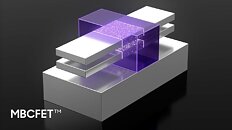
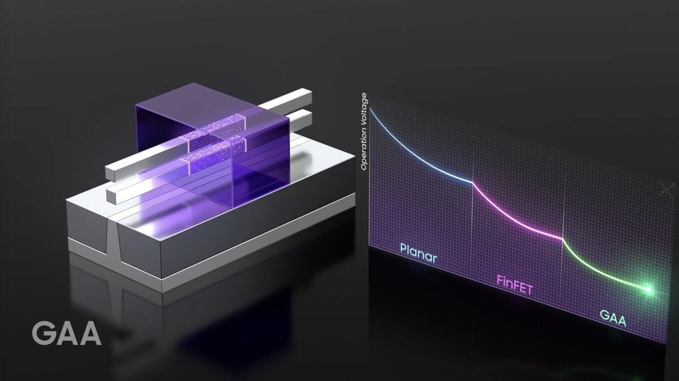
Samsung is determined in its plans to deliver the 3 nm silicon manufacturing process in the year 2022, and with it, there will be some major improvements to the transistor technology. We have already mentioned that Samsung is working on Gate-All-Around FET technology that will bring much better control of the transistor channel, preventing leakage at smaller nodes. However, today Samsung added a few more details about its upcoming Multi Bridge Channel FET technology for a 3 nm manufacturing process, simply called the MBCFET. Thanks to the report from Hardwareluxx, we have more details regarding the MBCFET technology and its characteristics.
Firstly, it is worth noting that MCBFET is a part of GAAFETs, meaning that the GAAFET is not one product, but rather a class of many based on its concepts. As far as the MCBFET performance goes, Samsung says that the technology will use 50% less power while delivering 30% more performance. There is going to be a big density gain as well, where Samsung predicts there will be around 45% less silicon space taken per one transistor. The comparison is made to an unspecified 7 nm process, possibly Samsung's process that uses FinFETs. The technology allows the stacking of transistors on top of each other, which makes it use inherently less space compared to regular FinFET. Being that MCBFET GAA transistors make its transistor width flexible, it means that the overall stacked transistor can be as wide as a designer needs it to be, adjusting for any scenario like low-power or high-performance.
Source:
Hardwareluxx
Firstly, it is worth noting that MCBFET is a part of GAAFETs, meaning that the GAAFET is not one product, but rather a class of many based on its concepts. As far as the MCBFET performance goes, Samsung says that the technology will use 50% less power while delivering 30% more performance. There is going to be a big density gain as well, where Samsung predicts there will be around 45% less silicon space taken per one transistor. The comparison is made to an unspecified 7 nm process, possibly Samsung's process that uses FinFETs. The technology allows the stacking of transistors on top of each other, which makes it use inherently less space compared to regular FinFET. Being that MCBFET GAA transistors make its transistor width flexible, it means that the overall stacked transistor can be as wide as a designer needs it to be, adjusting for any scenario like low-power or high-performance.

6 Comments on Samsung to Deliver 3 nm Manufacturing Process in 2022 with Next-Generation Transistors
the first picture shows the frequency difference between the very small 5nm nanowires, compared to the derivatives of the wider nanosheets with 15nm to 45nm width
the numbers by wich the different vendors can be compared are things like the gate pitch and such.
by using the nanowires and nanosheets even more areas with potential differences between the vendors have to be recognised in those comparisons.
there are (like ever) points of common knowledge and points of differences in the vendors strategies to a final product.
as an enduser the only things i would care about are, perf/watt, absolute perf and the powerfootprint regarding the formfactor of the targetmarket.