News Posts matching #2026

Return to Keyword Browsing

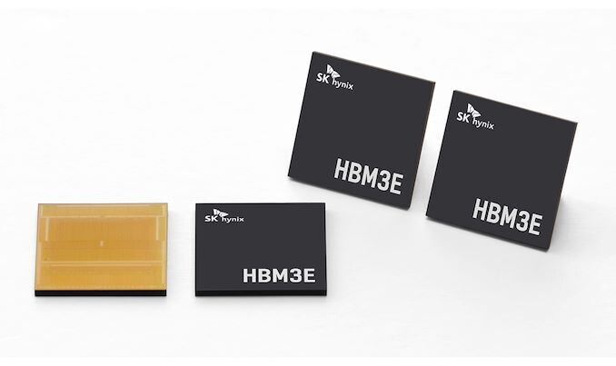
JEDEC Agrees to Relax HBM4 Package Thickness

JEDEC is currently presiding over standards for 6th generation high bandwidth memory (AKA HBM4)—the 12 and 16-layer DRAM designs are expected to reach mass production status in 2026. According to a ZDNET South Korea report, involved manufacturers are deliberating over HBM4 package thicknesses—allegedly, decision makers have settled on 775 micrometers (μm). This is thicker than the previous generation's measurement of 720 micrometers (μm). Samsung Electronics, SK Hynix and Micron are exploring "hybrid bonding," a new packaging technology—where onboard chips and wafers are linked directly to each other. Hybrid bonding is expected to be quite expensive to implement, so memory makers are carefully considering whether HBM4 warrants its usage.

ZDNET believes that JEDEC's agreement—settling on 775 micrometers (μm) for 12-layer and 16-layer stacked HBM4—could have: "a significant impact on the future packaging investment trends of major memory manufacturers. These companies have been preparing a new packaging technology, hybrid bonding, keeping in mind the possibility that the package thickness of HBM4 will be limited to 720 micrometers. However, if the package thickness is adjusted to 775 micrometers, 16-layer DRAM stacking HBM4 can be sufficiently implemented using existing bonding technology." A revised schedule could delay the rollout of hybrid bonding—perhaps pushed back to coincide with a launch of seventh generation HBM. The report posits that Samsung Electronics, SK Hynix and Micron memory engineers are about to focus on the upgrading of existing bonding technologies.

Samsung Accelerates R&D of Glass Substrate Chip Packaging

The Samsung Group has formed a new cross-department alliance—according to South Korea's Sedaily—this joint operation will concentrate on the research and development of a "dream substrate." The company's Electronics, Electrical Engineering, and Display divisions are collaborating in order to accelerate commercialization of "glass substrate" chip packaging. Last September, Intel revealed its intention to become an industry leader in "glass substrate production for next-generation advanced packaging." Team Blue's shiny new Arizona fabrication site will be taking on this challenge, following ten years of internal R&D work. Industry watchdogs reckon that mass production—in North America—is not expected to kick off anytime soon. Sensible guesstimates suggest a start date somewhere in 2030.

The Sedaily article states that Samsung's triple department alliance will target "commercialization faster than Intel." Company representatives—in attendance at CES 2024—set a 2026 window as their commencement goal for advanced glass substrate chip package mass production. An unnamed South Korean industry watcher has welcomed a new entrant on the field: "as each company possesses the world's best technology, synergies will be maximized in glass substrate research, which is a promising field...it is also important to watch how the glass substrate ecosystem of Samsung's joint venture will be established." Glass substrate packaging is ideal for "large-area and high-performance chip combinations" due to inherent heat-resistant properties and material strength. So far, the semiconductor industry has struggled with its development—hence the continued reliance on plastic boards and organic materials.

Apple Reportedly Developing 20.3-inch Foldable MacBook for 2027 Launch

According to renowned Apple analyst Ming-Chi Kuo, Apple is actively working on a foldable 20.3-inch MacBook, with mass production expected to begin in 2027. In a recent post on X/Twitter, Kuo stated that this foldable MacBook is currently Apple's only foldable product with a clear development schedule. Kuo's revelation comes amidst frequent inquiries about whether Apple plans to mass-produce a foldable iPhone or iPad in 2025 or 2026. His latest survey indicates that while Apple may explore these options, the foldable MacBook is the only device with a definitive timeline. This is not the first time rumors have circulated about a potential foldable MacBook from Apple. In 2022, display industry analyst Ross Young and Bloomberg's Mark Gurman both reported that Apple was interested in launching a foldable device with a screen size of around 20 inches.

Details about the foldable MacBook's design remain scarce, but it is expected to feature a single foldable OLED display that can be used in various configurations, such as a laptop mode with a virtual keyboard on the lower half of the screen or as a large tablet when fully unfolded. While competitors like Samsung, Motorola, and Huawei have already released foldable smartphones, Apple appears to be more cautious, focusing on perfecting the technology before bringing a product to market. As the foldable device market evolves, it will be interesting to see how Apple's unique take on the form factor fares. As Apple's first foldable product, it will be interesting to see what design choices are made and what hardware configuration will be present. But we are still relatively far away from the actual release of 2027.

ASML High-NA EUV Twinscan EXE Machines Cost $380 Million, 10-20 Units Already Booked

ASML has revealed that its cutting-edge High-NA extreme ultraviolet (EUV) chipmaking tools, called High-NA Twinscan EXE, will cost around $380 million each—over twice as much as its existing Low-NA EUV lithography systems that cost about $183 million. The company has taken 10-20 initial orders from the likes of Intel and SK Hynix and plans to manufacture 20 High-NA systems annually by 2028 to meet demand. The High-NA EUV technology represents a major breakthrough, enabling an improved 8 nm imprint resolution compared to 13 nm with current Low-NA EUV tools. This allows chipmakers to produce transistors that are nearly 1.7 times smaller, translating to a threefold increase in transistor density on chips. Attaining this level of precision is critical for manufacturing sub-3 nm chips, an industry goal for 2025-2026. It also eliminates the need for complex double patterning techniques required presently.

However, superior performance comes at a cost - literally and figuratively. The hefty $380 million price tag for each High-NA system introduces financial challenges for chipmakers. Additionally, the larger High-NA tools require completely reconfiguring chip fabrication facilities. Their halved imaging field also necessitates rethinking chip designs. As a result, adoption timelines differ across companies - Intel intends to deploy High-NA EUV at an advanced 1.8 nm (18A) node, while TSMC is taking a more conservative approach, potentially implementing it only in 2030 and not rushing the use of these lithography machines, as the company's nodes are already developing well and on time. Interestingly, the installation process of ASML's High-NA Twinscan EXE 150,000-kilogram system required 250 crates, 250 engineers, and six months to complete. So, production is as equally complex as the installation and operation of this delicate machinery.

SK Hynix Targets HBM3E Launch This Year, HBM4 by 2026

SK Hynix has unveiled ambitious High Bandwidth Memory (HBM) roadmaps at SEMICON Korea 2024. Vice President Kim Chun-hwan announced plans to mass produce the cutting-edge HBM3E within the first half of 2024, touting 8-layer stack samples already supplied to clients. This iteration makes major strides towards fulfilling surging data bandwidth demands, offering 1.2 TB/s per stack and 7.2 TB/s in a 6-stack configuration. VP Kim Chun-hwan cites the rapid emergence of generative AI, forecasted for 35% CAGR, as a key driver. He warns that "fierce survival competition" lies ahead across the semiconductor industry amidst rising customer expectations. With limits approaching on conventional process node shrinks, attention is shifting to next-generation memory architectures and materials to unleash performance.

SK Hynix has already initiated HBM4 development for sampling in 2025 and mass production the following year. According to Micron, HBM4 will leverage a wider 2048-bit interface compared to previous HBM generations to increase per-stack theoretical peak memory bandwidth to over 1.5 TB/s. To achieve these high bandwidths while maintaining reasonable power consumption, HBM4 is targeting a data transfer rate of around 6 GT/s. The wider interface and 6 GT/s speeds allow HBM4 to push bandwidth boundaries significantly compared to prior HBM versions, fueling the need for high-performance computing and AI workloads. But power efficiency is carefully balanced by avoiding impractically high transfer rates. Additionally, Samsung is aligned on a similar 2025/2026 timeline. Beyond pushing bandwidth boundaries, custom HBM solutions will become increasingly crucial. Samsung executive Jaejune Kim reveals that over half its HBM volume already comprises specialized products. Further tailoring HBM4 to individual client needs through logic integration presents an opportunity to cement leadership. As AI workloads evolve at breakneck speeds, memory innovation must keep pace. With HBM3E prepping for launch and HBM4 in the plan, SK Hynix and Samsung are gearing up for the challenges ahead.

Intel Reportedly Selects TSMC's 2 Nanometer Process for "Nova Lake" CPU Generation

A Taiwan Economic Daily news article proposes that a couple of high profile clients are considering TSMC's 2 nanometer process—Apple is widely believed to be the first customer to join the foundry's queue for cutting edge services. The report posits that Intel is also signed up on the Taiwanese firm's 2 nm reservation list—TSMC is expected to start production in 2025—insiders reckon that Team Blue's "Nova Lake" CPU family is the prime candidate here. Its CPU tile is alleged to utilize TSMC 2 nm node. Intel's recent "Core" processor roadmaps do not display any technologies beyond 2025—many believe that "Nova Lake" is pencilled in for a loose 2026 launch window, perhaps within the second half of the year.

The existence of "Nova Lake" was revealed late last year by HWiNFO patch notes—a short entry mentioned preliminary support for the family's integrated GPU. Intel is engaged in hyping up of its own foundry's 20A and 18A processes, but remain reliant on TSMC plants for various bits of silicon. Industry tipsters reckon that aspects of "Lunar Lake" CPUs are based on the Taiwanese foundry's N3B node. Team Blue Corporation and United Microelectronics Corporation (UMC) announced a new development partnership last week, but initial offerings will arrive on a relatively passé "12-nanometer semiconductor process platform." TSMC's very advanced foundry services seem to be unmatched at this juncture.

Apple to Become the First and Largest Customer of Amkor's Arizona Chip Packaging Plant

Apple has announced a partnership deal with Amkor, one of the leading chip packaging and testing manufacturers, which will build a two billion US Dollar silicon packaging facility in Peoria, Arizona. Being the only US-based OSAT (outsourced semiconductor assembly and test) provider, Amkor has decided to invest its funds and apply for the CHIPS Act, hoping to get a part of the funding from the US government's grant budget. The state-of-the-art facility in Arizona will feature over 500,000 square feet (46,452 square meters) of cleanroom space for packaging and testing chips. Using Amkor's latest technologies, the plant will support advanced computing, automotive, and communications chip packaging. It is tailored to meet the capacity needs of major customer Apple starting in 2025-2026. Apple will be the largest customer, with the Amkor facility packaging Apple-designed chips produced at the nearby TSMC wafer fabrication plant.

Building a chip packaging facility in the US with advanced packaging types means that the domestic manufacturing of advanced silicon is now possible across almost the entire supply chain, with OSAT now being present on US soil as well. In the initial phase, this partnership will enable domestic advanced packaging capabilities for leading-edge chips down to 3 nm nodes, which Apple plans to utilize for its A and M series of processors. Along with the creation of an estimated 2,000 local jobs, the investment serves as a boost to the local economy as well. Additionally, Amkor is TSMC's strategic partner, meaning future designs and packaging will cooperate without any delays.

Semiconductor Market to Grow 20.2% in 2024 to $633 Billion, According to IDC

International Data Corporation (IDC) has upgraded its Semiconductor Market Outlook by calling a bottom and return to growth that accelerates next year. IDC raised its September 2023 revenue outlook from $518.8 billion to $526.5 billion in a new forecast. Revenue expectations for 2024 were also raised from $625.9 billion to $632.8 billion as IDC believes the U.S. market will remain resilient from a demand standpoint and China will begin recovering by the second half of 2024 (2H24).

IDC sees better semiconductor growth visibility as the long inventory correction subsides in two of the largest market segments: PCs and smartphones. Automotive and Industrials elevated inventory levels are expected to return to normal levels in 2H24 as electrification continues to drive semiconductor content over the next decade. Technology and large flagship product introductions will drive more semiconductor content and value across market segments in 2024 through 2026, including the introduction of AI PCs and AI Smartphones next year and a much-needed improvement in memory ASPs and DRAM bit volume.

ASML to Add 600 DUV Machines to China's Semiconductor Manufacturing Capacity by 2025

Thanks to the TMTPost interview with the Global Vice President and China President of ASML, Shen Bo, the Dutch semiconductor equipment manufacturer has revealed that around 1,400 of its deep ultraviolet (DUV) lithography and metrology machines are currently installed in China. The company is expected to achieve a global output of 600 DUV equipment units by the end of 2025. Shen Bo stated that the company aims to install 500-600 units of DUV machinery in China by late 2025 or early 2026. The growth in ASML's Chinese revenues was notably high, with China contributing 46% of the company's system sales in 3Q 2023, representing an 82% revenue increase from the previous quarter.

China plans to build 25 12-inch wafer fabs in the next five years, covering logic wafers, DRAM, and MEMS production. ASML currently has a substantial presence in China, with 16 offices, 12 warehouses, distribution centers, development centers, training centers, and maintenance centers. The company employs over 1,600 people for its China operations. Despite the export restrictions imposed by the US government, ASML anticipates that the new measures will have little impact on its financial outlook for 2023 as it strives to meet the growing demand for semiconductor manufacturing equipment in the global market.

Fujitsu Details Monaka: 150-core Armv9 CPU for AI and Data Center

Ever since the creation of A64FX for the Fugaku supercomputer, Fujitsu has been plotting the development of next-generation CPU design for accelerating AI and general-purpose HPC workloads in the data center. Codenamed Monaka, the CPU is the latest creation for TSMC's 2 nm semiconductor manufacturing node. Based on Armv9-A ISA, the CPU will feature up to 150 cores with Scalable Vector Extensions 2 (SVE2), so it can process a wide variety of vector data sets in parallel. Using a 3D chiplet design, the 150 cores will be split into different dies and placed alongside SRAM and I/O controller. The current width of the SVE2 implementation is unknown.

The CPU is designed to support DDR5 memory and PCIe 6.0 connection for attaching storage and other accelerators. To bring cache coherency among application-specific accelerators, CXL 3.0 is present as well. Interestingly, Monaka is planned to arrive in FY2027, which starts in 2026 on January 1st. The CPU will supposedly use air cooling, meaning the design aims for power efficiency. Additionally, it is essential to note that Monaka is not a processor that will power the post-Fugaku supercomputer. The post-Fugaku supercomputer will use post-Monaka design, likely iterating on the design principles that Monaka uses and refining them for the launch of the post-Fugaku supercomputer scheduled for 2030. Below are the slides from Fujitsu's presentation, in Japenese, which highlight the design goals of the CPU.

TSMC Could Delay 2 nm Mass Production to 2026

According to TechNews.tw, TSMC could postpone its 2 nm semiconductor manufacturing node for 2026. If the rumors about TSMC's delayed 2 nm production schedule are accurate, the implications could reverberate throughout the semiconductor industry. TSMC's alleged hesitancy could be driven by multiple factors, including the architectural shift from FinFET to Gate-All-Around (GAA) and potential challenges related to scaling down to 2 nm. The company is a crucial player in this space, and a delay could offer opportunities for competitors like Samsung, which has already transitioned to GAA transistor architecture for its 3 nm chips. Given the massive demand for advanced nodes due to the rise of AI, IoT, and other next-gen technologies, it is surprising to hear "sluggish" demand reports.

However, it's also possible that it's too early for customers to make firm commitments for 2025 and beyond. TSMC has dismissed these rumors, stating that construction is progressing according to plan, which includes having 2 nm pilot run in 2024, and mass production in the second half of 2025.. Despite this, any delay in TSMC's roadmap could serve as a catalyst for shifts in market dynamics. Companies that rely heavily on TSMC's advanced nodes might need to reassess their timelines and strategies. Moreover, if Samsung can capitalize on this opportunity, it could somewhat level the playing field. As of now, though, it's essential to approach these rumors with caution until more concrete information becomes available.

Leak Suggests AMD 6th Gen EPYC "Venice" CPUs Linked to New SP7 Socket

Hardware leaker, YuuKi_AnS, has briefly turned their attention away from all things Team Blue—their latest leak points to upcoming server-grade processors chez AMD. A Zen 6 core-based 9006 EPYC CPU series, codenamed "Venice," is expected to arrive within two to three years along with an all-new SP7 socket—this information seems to have been sourced from an unnamed server manufacturer's product roadmap. A partial view of said slide also reveals forthcoming equipment powered by Intel "Falcon Shore" and NVIDIA "Blackwell" GPU technologies.

As reported a couple of months ago, older insider info has AMD using "Weisshorn" as an in-house moniker for Zen 6 "Morpheus" architecture, destined for Venice CPUs—alleged to form part of a 2025/2026 EPYC lineup. YuuKi_AnS proposes that these will utilize either 12-channel or 16-channel DDR5 memory configurations—thus providing plenty of bandwidth across hundreds of Zen cores. Altogether very handy for cloud, enterprise, and HPC workloads—industry experts reckon that 384-core counts are feasible on single packages. Naturally, a Team Red timeline dictates that Zen 5 "Nirvana" is due before Zen 6 "Morpheus," so EPYC 9005 "Turin(-X)" and 8005 "Turin-Dense" lineups are (allegedly) up for a 2024-ish launch window on SP5 (LGA-6096) and SP6 (LGA 4094) socket types.

JPR: PC GPU Shipments increased by 11.6% Sequentially from Last Quarter and Decreased by -27% Year-to-Year

Jon Peddie Research reports the growth of the global PC-based graphics processor unit (GPU) market reached 61.6 million units in Q2'23 and PC CPU shipments decreased by -23% year over year. Overall, GPUs will have a compound annual growth rate of 3.70% during 2022-2026 and reach an installed base of 2,998 million units at the end of the forecast period. Over the next five years, the penetration of discrete GPUs (dGPUs) in the PC will grow to reach a level of 32%.

Year to year, total GPU shipments, which include all platforms and all types of GPUs, decreased by -27%, desktop graphics decreased by -36%, and notebooks decreased by -23%.

Leaked Intel Roadmap Casts Doubt on Meteor Lake-S Desktop CPU Lineup

The fate of Intel's Meteor Lake-S desktop CPU lineup has been the topic of much debate since the end of last year - at the time, industry tipsters proposed that part of the product range had been disposed of entirely, but several leaks throughout the course of 2023 have indicated that MTL-S processors were on-track for a launch later in the year - albeit restricted to i3 and i5 offerings. An Intel employee has also confirmed that a new SKU naming system will be implemented as part of the upcoming Meteor Lake lineup - although he did not clarify whether this would encompass both mobile and desktop variants.

An alleged Intel client CPU roadmap has made its way onto the internet, and tipsters think that the information on hand shows that Team Blue has pulled the plug on its Meteor Lake-S (6 Performance and 8 Efficiency cores) desktop processors. The presentation slide was likely authored earlier this month - so these developments are relatively fresh, with provisions for Core S, H, PX, M, U & N series. The heavily redacted infographic maps out product release windows going as far forward as Q4 2026. OneRaichu posits that an Arrow Lake-S (6P + 8E) CPU lineup will replace MTL-S. It is possible that Intel's Raptor Lake-S refresh could serve as an interim release this year, since the Arrow Lake generation is expected to arrive in 2024.

US Government Targeting Crypto Miners With Proposed Energy Bill Tax

The US Government is considering new plans that will attempt to curb the after effects of cryptocurrency mining. The White House revealed details about its proposed "DAME Tax" scheme on Tuesday of this week - the Digital Asset Mining Energy excise tax is under consideration for this year's US Budget. The government wants to address the impact that cryptomining has on the US economy as well as the environment, alongside numerous other national challenges. Companies engaged in the extraction of cryptocurrencies could be charged extra for the running of computer equipment (starting in early 2024). A White House spokesperson states: "after a phase-in period, firms would face a tax equal to 30 percent of the cost of the electricity they use in cryptomining."

American crypto companies are facing a 10 percent taxation of their energy bill for 2024, that will then increase to 20 percent in 2025, and the maximum tax rate will hit a high of 30 percent in 2026. The White House number crunching team reckons that $3.5 billion could be generated by the proposed DAME excise tax. The new rules would represent a radical change for large scale cryptomining efforts: "Currently, cryptomining firms do not have to pay for the full cost they impose on others, in the form of local environmental pollution, higher energy prices, and the impacts of increased greenhouse gas emissions on the climate. The DAME tax encourages firms to start taking better account of the harms they impose on society," reads a White House statement." The government's investigation has determined that the domestic cryptomining industry is close to consuming more electricity than the entire nation's residential lighting system. US lawmakers last year calculated that some of the larger digital asset mining firms are capable of using more energy than nearly all of the residential population based in Houston, TX.
Return to Keyword Browsing
May 1st, 2024 07:36 EDT change timezone

New Forum Posts

Popular Reviews

Controversial News Posts