News Posts matching #28 nm

Return to Keyword Browsing

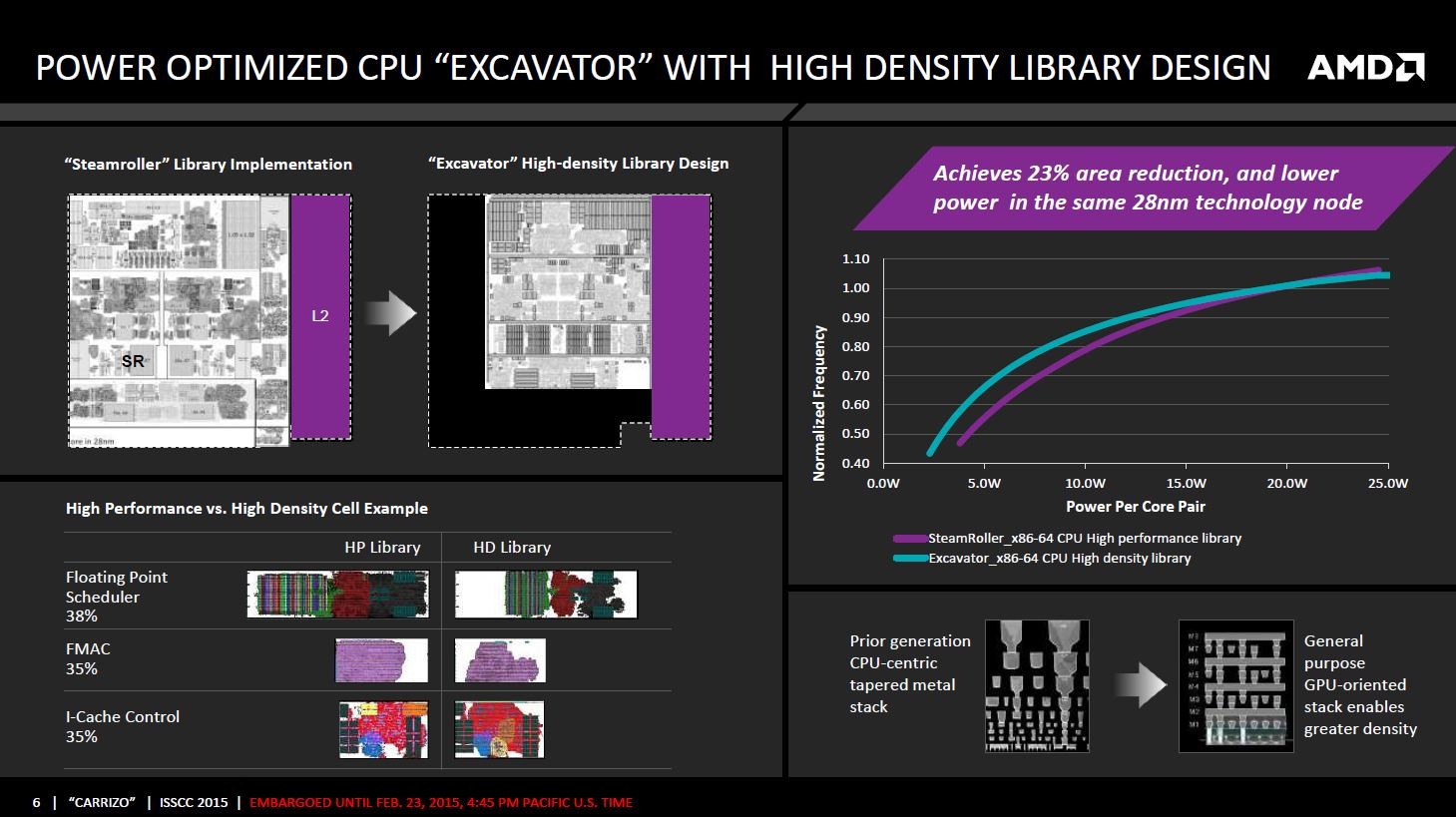
GIGABYTE Intros its GeForce GTX 960 ITX Graphics Card

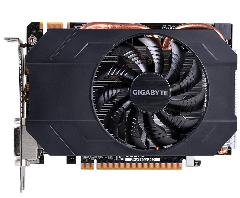
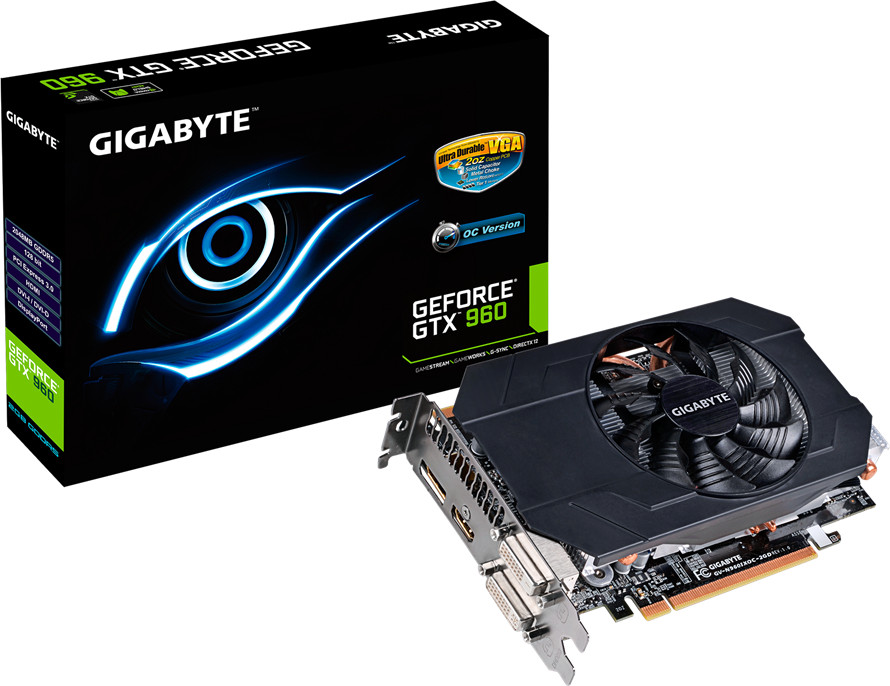
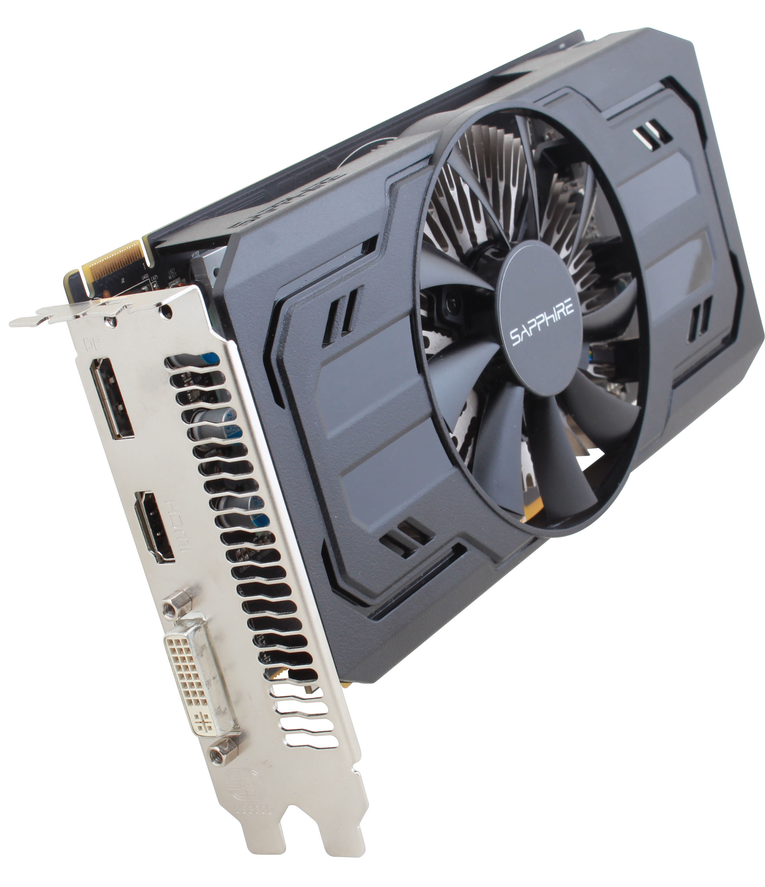
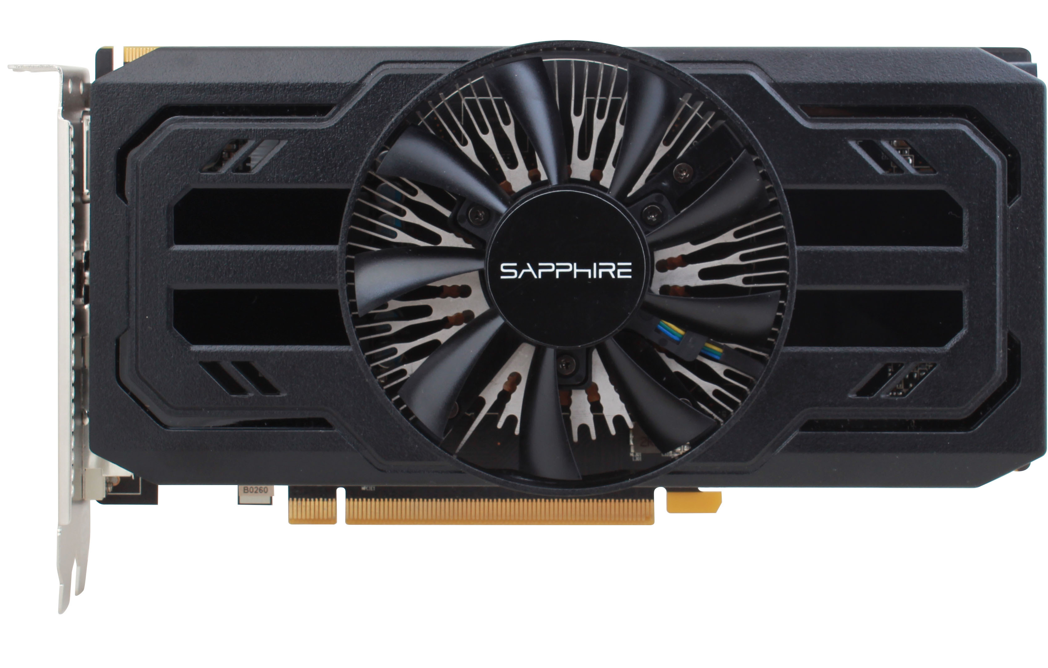
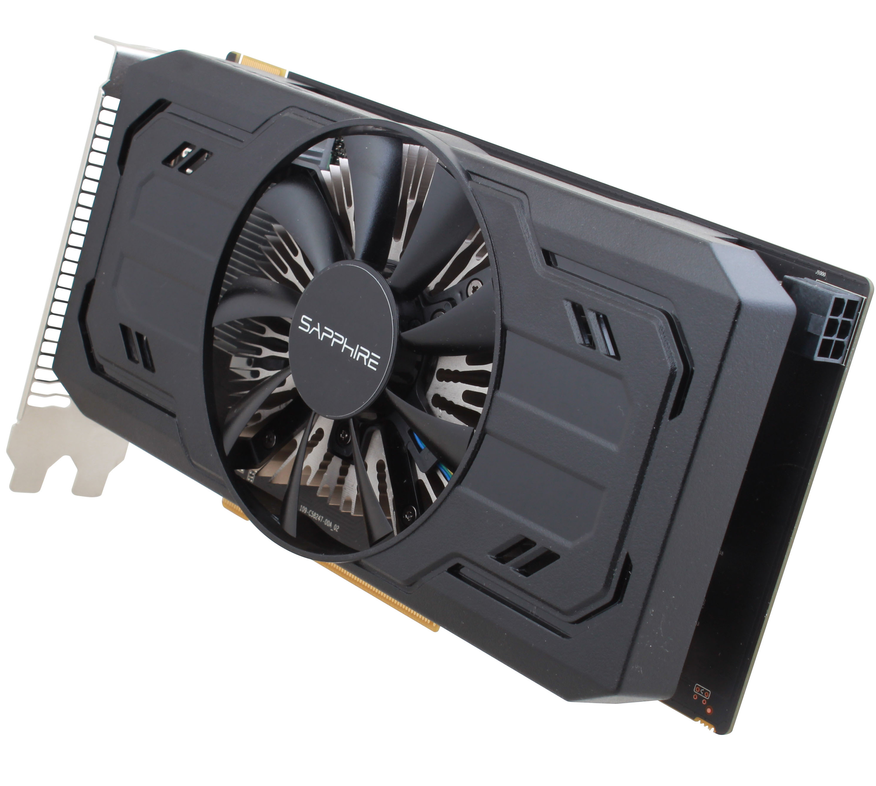
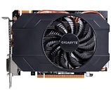
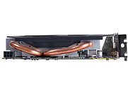
GIGABYTE rolled out its latest GeForce GTX 960, designed for space-constrained builds, the GV-N960IX-2GD. This full-height graphics card is just 18.1 cm long, and should squeeze into most compact cubical ITX cases. It features a custom-design PCB that draws power from a single 6-pin PCIe power connector; mated to a compact single-fan cooling solution, which uses a single 90 mm fan to ventilate a dense aluminium fin heatsink, to which heat drawn directly from the GPU die is fed by a pair of 8 mm thick copper heat pipes.

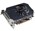
The card offers out of the box clock speeds of 1127 MHz core, 1178 MHz GPU Boost, and 7.00 GHz memory (all reference), and features 2 GB of GDDR5 memory across the chip's 128-bit wide memory interface. Display outputs include a pair of dual-link DVI connectors, and one each of HDMI 2.0 and DisplayPort 1.2. Based on the 28 nm GM206 silicon, the GeForce GTX 960 features 1,024 CUDA cores based on the "Maxwell" architecture. The company didn't announce pricing or availability information.

NVIDIA GeForce GTX TITAN-X Specs Revealed

NVIDIA's GeForce GTX TITAN-X, unveiled last week at GDC 2015, is shaping up to be a beast, on paper. According to an architecture block-diagram of the GM200 silicon leaked to the web, the GTX TITAN-X appears to be maxing out all available components on the 28 nm GM200 silicon, on which it is based. While maintaining the same essential component hierarchy as the GM204, the GM200 (and the GTX TITAN-X) features six graphics processing clusters, holding a total of 3,072 CUDA cores, based on the "Maxwell" architecture.

With "Maxwell" GPUs, TMU count is derived as CUDA core count / 16, giving us a count of 192 TMUs. Other specs include 96 ROPs, and a 384-bit wide GDDR5 memory interface, holding 12 GB of memory, using 24x 4 Gb memory chips. The core is reportedly clocked at 1002 MHz, with a GPU Boost frequency of 1089 MHz. The memory is clocked at 7012 MHz (GDDR5-effective), yielding a memory bandwidth of 336 GB/s. NVIDIA will use a lossless texture-compression technology to improve bandwidth utilization. The chip's TDP is rated at 250W. The card draws power from a combination of 6-pin and 8-pin PCIe power connectors, display outputs include three DisplayPort 1.2, one HDMI 2.0, and one dual-link DVI.

ZOTAC Unveils a Pair of 4 GB GeForce GTX 960 Graphics Cards

ZOTAC joined the 4 GB GeForce GTX 960 party with two factory-overclocked models. The ZT-90308-10M features a minor overclock of 1177 MHz core, with 1240 MHz GPU Boost (vs. reference clocks of 1126/1178 MHz); while the AMP! variant (ZT-90309-10M) offers higher 1266 MHz core with 1329 MHz GPU Boost. The memory clock is untouched on both cards, at 7.00 GHz (GDDR5-effective).

The ZT-90308-10M features a more cost-effective dual-fan cooling solution, while the AMP! offers a meatier dual-fan one. Both cards draw power from single 8-pin PCIe power connectors, and come with back-plates. Display outputs on both include three DisplayPort 1.2, one HDMI 2.0, and one DVI. Based on the 28 nm GM206 silicon, the GTX 960 features 1,024 CUDA cores, 64 TMUs, 32 ROPs, and a 128-bit wide GDDR5 memory interface. ZOTAC didn't announce pricing or availability information.
More pictures follow.

NVIDIA GeForce GTX TITAN-X Pictured Up-close

Here are some of the first close-up shots of NVIDIA's new flagship graphics card, the GeForce GTX TITAN-X, outside Jen-Hsun Huang's Rafiki moment at a GDC presentation. If we were to throw in an educated guess, NVIDIA probably coined the name "TITAN-X" as it sounds like "Titan Next," much like it chose "TITAN-Z" as it sounds like "Titans" (plural, since it's a dual-GPU card). Laid flat out on a table, the card features an a matte-black colored reference cooling solution that looks identical to the one on the original TITAN. Other cosmetic changes include a green glow inside the fan intake, the TITAN logo, and of course, the green glow on the GeForce GTX marking on the top.

The card lacks a back-plate, giving us a peek at its memory chips. The card features 12 GB of GDDR5 memory, and looking at the twelve memory chips on the back of the PCB, with no other traces, we reckon the chip features a 384-bit wide memory interface. The 12 GB is achieved using twenty-four 4 Gb chips. The card draws power from a combination of 8-pin and 6-pin power connectors. The display I/O is identical to that of the GTX 980, with three DisplayPorts, one HDMI, and one DVI. Built on the 28 nm GM200 silicon, the GTX TITAN-X is rumored to feature 3,072 CUDA cores. NVIDIA CEO claimed that the card will be faster than even the previous generation dual-GPU flagship product by NVIDIA, the GeForce GTX TITAN-Z.

Sapphire Rolls Out Radeon R7 260X iCafe OC Graphics Card

Sapphire rolled out the entry-mid range Radeon R7 260X iCafe OC graphics card for casual-gaming PC builds (eg: low-cost Counter Strike gaming kiosks). Pictured below, the card looks rather premium, with its full-length, dual-slot cooler. That is, until you take a peek under its plastic shroud to find a cost-effective fan-heatsink cooling the GPU, with radially-projecting aluminium fins, a copper core base, and an 80 mm fan ventilating it.

The card draws power from a single 6-pin PCIe power connector; outputs include one each of dual-link DVI, HDMI 1.4a, and DisplayPort 1.2a. The card offers a factory-overclock of 1050 MHz core, and an untouched 5.00 GHz memory, against reference clocks of 1000 MHz on the core. Based on the 28 nm "Bonaire" silicon, the R7 260X offers 896 Graphics CoreNext stream processors, and a 128-bit wide GDDR5 memory interface, holding 2 GB of memory on this card. Expect a $100-ish pricing.

AMD's Excavator Core is Leaner, Faster, Greener

AMD gave us a technical preview of its next-generation "Carrizo" APU, which is perhaps the company's biggest design leap since "Trinity." Built on the 28 nm silicon fab process, this chip offers big energy-efficiency gains over the current-generation "Kaveri" silicon, thanks to some major under-the-hood changes.

The biggest of these is the "Excavator" CPU module. 23 percent smaller in area than "Steamroller," (same 28 nm process), Excavator features a new high-density library design, which reduces die-area of the module. Most components are compacted. The floating-point scheduler is 38% smaller, fused multiply-accumulate (FMAC) units compacted by 35%, and instruction-cache controller compacted by another 35%. The "Carrizo" silicon itself uses GPU-optimized high-density metal stack, which helps with the compaction. Each "Excavator" module features two x86-64 CPU cores, which are structured much in the same way as AMD's previous three CPU core generations.

AMD to Switch to GlobalFoundries' 28 nm SHP Node in 2015

Faced with continuous development roadblocks with TSMC, AMD is reportedly planning to switch to the 28 nm SHP process of GlobalFoundries, to build GPUs in 2015. The 28 nm SHP (super high-performance) node will allow the company to lower voltages, giving it greater room to increase clock speeds of its upcoming GPUs. AMD's GPUs in 2015 could be based on its latest Graphics CoreNext 1.2 architecture, and AMD needs every means to minimize voltages, and crank up clock speeds.

The company hasn't abandoned TSMC completely just yet, with reports speaking of AMD using the Taiwanese fab's 16 nm FinFet node to manufacture its next-generation "Zen" CPUs. Zen is the successor to AMD's "Bulldozer" architecture and its derivatives ("Piledriver" and "Steamroller.") It could feature a radically different core design.

Marvell Announces DRAM-less NVMe SSD Controller

Marvell, a worldwide leader in providing complete silicon solutions from mobile communications to storage, Internet of Things (IoT), cloud infrastructure, digital entertainment and in-home content delivery and Kinoma software enabling the "Smart Life and Smart Lifestyle," today announced the world's first DRAM-less NVMe (Non-Volatile Memory Express) solid state drive (SSD) controller for mass market mobile computing solutions with industry-leading NANDEdge low-density parity check (LDPC) technology supporting triple-level cell (TLC) and 3D NAND. Marvell's 88NV1140 and 88NV1120 enable small form factor SSD solutions with unparalleled performance for integration into low-z-height tablets, Chrome devices and the upcoming wave of new 2-in-1 hybrid/detachable mobile PC platforms.

"As mobile computing and cloud-based services become an integral part of our daily lives, fast, secure, reliable and cost effective storage solutions with a small form factor are the key to bringing the benefit of technology to the mass market. I believe our latest game-changing SSD controller will drive the fast deployment of a new wave of small form factor SSD solutions for the mass market mobile computing platforms," said Weili Dai, President and Co-Founder of Marvell. "I am very pleased to see Marvell's leadership and our long track record of invention and innovation including the world's first DRAM-less NVMe SSD controller and the industry's most advanced LDPC technology enabling the latest TLC and 3D NAND flash memory. I am very thankful for our global engineering teams who continuously raise the technology bar to move our industry forward faster."

NVIDIA GeForce GTX TITAN II Detailed

Riding on the success of its GM204 silicon, it looks like NVIDIA won't wait for the 20 nm silicon fab process to build its next big GPU, which powers its enthusiast-segment graphics cards. The GM200 silicon will be built on the existing 28 nm silicon fab process. Among other SKUs, NVIDIA's next GeForce GTX TITAN product, the GTX TITAN II, could be based on this chip. A curious-looking data entry was submitted from an anonymous source to SiSoft's hardware database, which gives away some rather glaring details of the GM200.

To begin with, the GM200 will be built on the existing 28 nm node, and will feature a die-area of 551 mm². The chip will be based on the "Maxwell" architecture, and feature 3,072 CUDA cores, cushioned by a 3 MB L3 cache. The chip will likely feature a 384-bit wide GDDR5 memory interface, with lossless texture compression algorithms, which work to step up memory bandwidth. The standard memory amount is a staggering 12 GB, double that of the first-generation GTX TITAN. Given how AMD recently gave 8 GB variants of its Radeon R9 290X a coordinated launch, GPU vendors could be seeing a utility in giving their products such massive amounts of video memory, to cope with resolutions such as 4K Ultra HD, and perhaps even 5K 16xHD. The chip features reasonably high clock speeds, with the core running at 1100 MHz, and a staggering 1390 MHz GPU Boost. The memory, however, is clocked at 6.00 GHz.

Radeon R9 290X Sees Price Cuts

AMD is apparently working with its add-in board manufacturers and retailers to bring down prices of its flagship single-GPU graphics card, the Radeon R9 290X. The card can now be had for as low as $449, non-reference design, factory-overclocked cards starting at a $50 premium. Prices could settle down somewhere between $450 and $500. This closely follows AMD's move to bring down price of its dual-GPU flagship Radeon R9 295X2 by a whopping 34 percent, down to $999, offering performance competitive to the $2999 GeForce GTX TITAN-Z. NVIDIA is preparing two new graphics cards competitive in performance to the Radeon R9 290 series, the GeForce GTX 970 and GTX 980. The two are based on the company's new 28 nm "GM204" silicon, implementing the "Maxwell" GPU architecture.

MSI Teases GeForce GTX 970 Gaming with TwinFrozr V

MSI showed off the first moneyshot render of its GeForce GTX 970 Gaming graphics card. Trailing an earlier leaked render viewed from the top of the card. The new one reveals MSI giving the TwinFrozr V cooler a bold 2-tone cooler shroud, holding a pair of 100 mm fans that ventilate a chunky copper heat-pipe fed aluminium fin stack. MSI could give the GTX 970 a factory-overclock to take advantage of its meaty cooling solution. Based on the 28 nm GM204 silicon, the GeForce GTX 970 is said to feature 1,664 CUDA cores based on the "Maxwell" architecture, 138 TMUs, 32 ROPs, a 256-bit wide memory interface, and 4 GB of memory. It will launch a little later this month.

XFX Radeon R9 285 Pictured, Too

In addition to a Sapphire-branded Radeon R9 285, pictures of an XFX branded one surfaced, too. The Radeon R9 285 is a new SKU being designed by AMD to take on the GeForce GTX 760 in not just performance, but also energy efficiency. It's rumored to be based on a brand new 28 nm silicon, codenamed "Tonga," which features GCN2 stream processor count identical to one of the variants of "Tahiti," and a 256-bit wide memory interface. The card thus features 2 GB of memory. XFX gave its card its signature Double Dissipation (DD) cooling solution.

Marvell Introduces the 88SS1093 PCIe 3.0 NVM Express SSD Controller

Marvell today announced the introduction of its first native Non-Volatile Memory Express (NVMe) solid-state drive (SSD) controller, the 88SS1093. The Marvell 88SS1093 NVMe SSD controller delivers high-performance solid-state storage solutions with a fully Flash-optimized architecture overcoming the SAS/SATA performance limitations by optimizing hardware and software to take full advantage on NAND and addressing the needs of data centers and client systems that utilize next-generation PCIe 3.0 SSD storage. The 88SS1093 also integrates Marvell's third generation NANDEdge error-correcting, low-density parity check (LDPC) technology for higher reliability and endurance boost that was previously announced with Marvell's fifth generation SATA SSD controller, the 88SS1074.

"As the global leader of the storage industry, we are very proud of our innovation, invention, and contribution to the advancement of a wide range of storage technologies and products. I am very excited to see that our new SSD controller solution has once again raised the technology bar with superior performance, high reliability and robust security," said Weili Dai, President and Co-Founder of Marvell. "I am very proud of our close collaboration with leading tier one OEM and ODM partners around the world in enabling the rapid growth of the SSD market from client devices to data centers and enterprise systems. At Marvell, it is our pride and long term commitment to drive innovation to better lives for all in the new era of 'Smart Life and Smart Lifestyle'."

AMD Announces the Athlon 860K and FX-8300 CPUs

In addition to its new A-series APUs, AMD announced two new CPUs, the Athlon 860K, and the FX-8300. Built in the FM2+ package, the Athlon 860K is a quad-core CPU based on the 28 nm "Kaveri" silicon, with its integrated graphics disabled. It features four "Steamroller" CPU cores clocked at 3.70 GHz, with an unlocked base-clock multiplier that enables overclocking. The two modules that make up the four cores feature half their normal L2 cache amounts, and so the total L2 cache is just 2 MB. The chip will run on socket FM2+ motherboards based on the A88X, A85, A75, and A55 chipsets. The FX-8300, on the other hand, is a budget eight-core processor in the AM3+ package. It's based on the 32 nm "Vishera" silicon, featuring eight CPU cores spread across four "Piledriver" modules; clocked at 3.20 GHz, with 3.50 GHz of Turbo Core frequencies. The chips feature 2 MB of L2 cache per module, and 8 MB of shared L3 cache. Its TDP is rated at 95W.

NVIDIA Moving Around the Fabled GeForce GTX TITAN II

NVIDIA is moving around engineering samples of what it describes as "GM200 A1 graphics processor," in its shipping manifest. The sample was making its way from Taiwan, to Bangalore, India, from where it's likely pushed to the company's facilities in Bangalore and Hyderabad. A1 steppings of NVIDIA chips are usually pre-production, and bound for just a few more rounds of testing, before being upgraded to "A2" and mass-produced. German tech site 3DCenter.org also pulled out some likely specifications from its sources.

To begin with, the GM200, like the GM204, will be built on existing 28 nm silicon fabrication process, as both NVIDIA and AMD appear to have suffered design setbacks due to their common foundry partner, TSMC, not being able to set its next-gen 20 nm node up to speed in time. The GM200 is expected to feature over 4,000 CUDA cores, although the exact number is unknown. It is expected to widen the memory bus to 512-bit. Given the existing process, the GPU will be huge. Over 600 mm² huge. NVIDIA will probably bank on the energy efficiency of its "Maxwell" architecture to cope with thermal loads put out by a chip that big. The GM200-based "GeForce GTX TITAN II" could launch in the first half of 2015.

NVIDIA GeForce GTX 880 and GTX 870 to Launch This Q4

NVIDIA is planning to launch its next high performance single-GPU graphics cards, the GeForce GTX 880 and GTX 870, no later than Q4-2014, in the neighborhood of October and November, according to a SweClockers report. The two will be based on the brand new "GM204" silicon, which most reports suggest, is based on the existing 28 nm silicon fab process. Delays by NVIDIA's principal foundry partner TSMC to implement its next-generation 20 nm process has reportedly forced the company to design a new breed of "Maxwell" based GPUs on the existing 28 nm process. The architecture's good showing with efficiency on the GeForce GTX 750 series probably gave NVIDIA hope. When 20 nm is finally smooth, it wouldn't surprise us if NVIDIA optically shrinks these chips to the new process, like it did to the G92 (from 65 nm to 55 nm). The GM204 chip is rumored to feature 3,200 CUDA cores, 200 TMUs, 32 ROPs, and a 256-bit wide GDDR5 memory interface. It succeeds the company's current workhorse chip, the GK104.

Marvell Unveils the 88SS1074 SATA SSD Controller

Marvell today announced its game-changing fifth generation serial advanced technology attachment (SATA 6 Gb/s) solid-state drive (SSD) controller. The industry-leading Marvell 88SS1074 SATA SSD controller deploys Marvell's third generation NANDEdge error-correcting, low-density parity check (LDPC) technology, facilitating use of 15 nm triple-level cell (TLC) NAND flash in client and enterprise SSDs. The advanced SATA SSD controller significantly improves total storage system cost and delivers unparalleled performance with lower power consumption.

NVIDIA GM204 and GM206 to Tape-Out in April, Products to Launch in Q4?

It looks like things are going horribly wrong at TSMC, NVIDIA and AMD's principal foundry partner, with its 20 nm manufacturing process, which is throwing a wrench into the works at NVIDIA, forcing it to re-engineer an entire lineup of "Maxwell" GPUs based on existing 28 nm process. Either that, or NVIDIA is confident of delivering an efficiency leap using Maxwell on existing/mature 28 nm process, and saving costs in the process. NVIDIA is probably drawing comfort from the excellent energy-efficiency demonstrated by its Maxwell-based GeForce GTX 750 series. According to a 3DCenter.org report, NVIDIA's next mainline GPUs, the GM204 and GM206, which will be built on the 28 nm process, and "Maxwell" architecture, will tape out later this month. Products based on the two, however, can't be expected before Q4 2014, as late as December, or even as late as January 2015.

GM204 succeeds GK104 as the company's next workhorse performance-segment silicon, which could power graphics card SKUs ranging all the way from US $250 to $500. An older report suggests that it could feature as many as 3,200 CUDA cores. The GM204 could be taped out in April 2014, and the first GeForce products based on it could launch no sooner than December 2014. The GM206 is the company's next mid-range silicon, which succeeds GK106. It will tape out in April, alongside the GM204, but products based on it will launch only in January 2015. The GM200 is a different beast altogether. There's no mention of which process the chip will be based on, but it will succeed the GK110, and should offer performance increments worthy of being a successor. For that, it has to be based on the 20 nm process. It will tape-out in June 2014, and products based on it will launch only in or after Q2 2015.

AMD "Hawaii" Based Dual GPU Graphics Card Could be Named R9 295X2

AMD's dual-GPU flagship graphics card that runs a pair of 28 nm "Hawaii" GPUs is no unicorn, as the company began teasing the press about it. Dutch tech publication BouweenPC.nl dug up info that points to AMD naming the card "Radeon R9 295X2." The two "Hawaii" GPUs are expected to feature a core clock speed of no less than 1000 MHz, according to the report. It also adds that AMD is working on a air+liquid (hybrid) cooling solution for the card. Its cooler will feature heatsinks with a running air flow to cool the memory, VRM, and other hot ancillary components; while two liquid cooling blocks will dissipate heat form the GPUs. This would also mean that installing the R9 295X2 won't be as simple as pushing it into a PCIe slot, fastening a couple of screws, and plugging the PSU in. ASUS attempted a similar cooling solution for its Republic of Gamers ARES II graphics card.

GM107 Features 128 CUDA Cores Per Streaming Multiprocessor

NVIDIA's upcoming GM107 GPU, the first to be based on its next-generation "Maxwell" GPU architecture, reportedly features a different arrangement of CUDA cores and streaming multiprocessors to those typically associated with "Kepler," although the component hierarchy is similar. The chip reportedly features five streaming multiprocessors, highly integrated computation subunits of the GPU. NVIDIA is referring to these parts as "streaming multiprocessor (Maxwell)," or SMMs.

Further, each streaming multiprocessor features 128 CUDA cores, and not the 192 CUDA cores found in SMX units of "Kepler" GPUs. If true, GM107 features 640 CUDA cores, all of which will be enabled on the GeForce GTX 750 Ti. If NVIDIA is carving out the GTX 750 by disabling one of those streaming multiprocessors, its CUDA core count works out to be 512. NVIDIA will apparently build two GPUs on the existing 28 nm process, the GM107, and the smaller GM108; and three higher performing chips on the next-generation 20 nm process, the GM206, the GM204, and the GM200. The three, as you might have figured out, succeed the GK106, GK104, and GK110, respectively.

GTX 750 Taken Apart, Sips Power from a Single 6-pin Connector

Here are the first pictures of a partner-branded GeForce GTX 750 graphics card taken apart. It reveals a couple of things - to begin with, the GM107 silicon will bring about some genuine performance per Watt improvements, despite being based on the existing 28 nm silicon fab process, and second, that cards based on the chip will be extremely cheap to build, giving NVIDIA a good chance to strengthen its position in the sub-$200 market segment. This particular card is cooled by a simple fan-heatsink that's essentially a chunk of metal with a fan latched on to it. The card relies on a simple 2+1 phase VRM, which draws power from a single 6-pin PCIe power connector. NVIDIA is expected to launch the GTX 750 and GTX 750 Ti a little later this month.

GeForce GTX TITAN Black Pictured, Isn't Strictly Black

Here's the first alleged picture of NVIDIA's GeForce GTX TITAN Black, a high-end SKU NVIDIA is working on, to restore the competitiveness of the $999 price-point it commands. Although referred to as "TITAN Black," the card is nowhere close to looking like the CGI renders that surfaced last November. The board looks identical to the original GTX TITAN, except its "TITAN" etching on the cooler shroud is painted in black. The GTX TITAN Black maxes out the 28 nm GK110 silicon, featuring 2,880 CUDA cores, 240 TMUs, 48 ROPs, and a 384-bit wide GDDR5 memory interface, holding 6 GB of memory. It also features full DPFP for the GK110 silicon, which is exclusive to the GTX TITAN, within the GeForce range. NVIDIA is expected to give the GTX TITAN Black a low-key launch some time next week.

AMD Also Works on Radeon R9 280 to Heat Up Sub-$300 Segment

In addition to the Radeon R7 265, AMD is also planning to launch its 6th Radeon R9 series desktop discrete graphics card running up to Computex 2014, the Radeon R9 280. The R9 280, as some of you might have guessed by now, is based on the 28 nm "Tahiti" silicon, with a core-configuration identical to that of the Radeon HD 7950 from the previous generation, according to a WCCFTech report. The chip could hence feature 1,792 stream processors, 112 TMUs, 32 ROPs, and a 384-bit wide GDDR5 memory interface, holding 3 GB of memory.

The Radeon R9 280 could be clocked above 800 MHz on the core, and 5.00 GHz (GDDR5-effective) on the memory, which works out to 224 GB/s of memory bandwidth. Given that the R9 280X is still on paper a $299 SKU, AMD may intend the R9 280 to be priced within the sub-$300 segment. Beneath the R9 280X, AMD's GPUs are unappealing to crypto-currency miners as the performance-Watt and price-performance equations turn unfavorable, and so the R9 280 has a fair chance of sticking to its intended price-point, away from being wrecked by shamelessly greedy retailers.

NVIDIA GM107 "Maxwell" Silicon Pictured

Here is the first picture of a couple of NVIDIA GM107 silicons in a tray, ahead of graphics card assembly. The packages appear to be as big as those of the GK106 from the previous generation, however, the die itself is estimated to be smaller, at roughly 156 mm², compared to the 221 mm² die of the GK106, and the 118 mm² of the GK107. The best part? All three chips are built on the same 28 nm silicon fab process. So what makes the GM107 die smaller than that of the GK106 despite having a similar feature-set? Narrower memory bus. The GM107 is said to feature a 128-bit wide GDDR5 memory interface, in comparison to the 192-bit wide interface of the GK106.

Apart from the 128-bit wide GDDR5 memory interface, the GM107 is said to feature a total of 960 CUDA cores, 80 TMUs, and 16 ROPs. The CUDA core count is identical to that of the GK106. The GM107 is built on NVIDIA's next-generation "Maxwell" GPU architecture. It will form the foundation of two SKUs, the GeForce GTX 750 Ti, and the GeForce GTX 750. The former features the full complement of 960 CUDA cores; while the latter is slightly cut down, and features just 768. The TDP of the GTX 750 Ti is approximated to be around 75 Watt. If true, the GTX 750 duo will set new standards on the performance-per-Watt metrics. NVIDIA is expected to launch both, later this month.

GeForce GTX 750 Ti "Maxwell" First Performance Numbers Out

Ahead of its rumored mid-February launch, members of Taiwanese tech forum Coolaler.com posted the first performance benchmark numbers of the card. Originally thought to be positioned between the previous-generation GeForce GTX 660 and current GTX 760, the GTX 750 Ti, according to these numbers is on average 10 to 15 percent slower than the GTX 660, which should put its performance somewhere in between the GTX 650 Ti Boost and the GTX 660.

Then again, the testers must be using some very early drivers, and performance figures of the GTX 750 Ti should get clearer as its mid-February launch date approaches. The GeForce GTX 750 Ti is an important GPU for NVIDIA, as it's the first to be based on its next-generation "Maxwell" GPU micro-architecture. NVIDIA is trying the architecture out on current 28 nm process, before launching bigger chips based on the next-generation 20 nm fab process.
Return to Keyword Browsing
Jul 14th, 2025 15:57 CDT change timezone

New Forum Posts

Popular Reviews

TPU on YouTube

Controversial News Posts