News Posts matching #28 nm

Return to Keyword Browsing

NVIDIA Approaching Other Foundries than TSMC for 28 nm Production

NVIDIA, along with Qualcomm, is reportedly in talks with foundries other than TSMC, for manufacturing of its new 28 nm chips. Despite the fact that TSMC is ramping up its 28 nm capacity at a breakneck pace, NVIDIA is seeing a shortage of production that could affect its competitiveness. An interesting revelation here is that NVIDIA has begun sampling its GPUs on Samsung's 28 nanometer fab process. Samsung uses this process for contract-manufacturing of ARM application processors. Other foundries with proven 28 nm manufacturing capability include UMC.

TSMC 28 nm Capacity Ramp-Up Faster Than Older Processes

With launches of new-generation GPUs by NVIDIA and AMD, and new ARM application processor designs by various industry players, TSMC is under pressure to ramp up its production capacity for its new 28 nanometer note. DigiTimes research suggests that this ramp-up is going at a faster rate than older processes such as 40 nm and 65 nm nodes (when those were new). Digitimes Research analyst Nobunaga Chai claims that the 28 nm node started generating revenues in Q4, 2011, and sales ratio reached 5% in the following quarter. It is anticipated to see TSMC significantly ramp up its 28nm production capacity later in 2012, Chai believes.

ARM Announces Cortex-A15 Quad-Core Hard Macro

ARM today announced the availability of a high performance, power-optimized quad-core hard macro implementation of its flagship Cortex-A15 MPCore processor.

The ARM Cortex-A15 MP4 hard macro is designed to run at 2 GHz and delivers performance in excess of 20,000 DMIPS, while maintaining the power efficiency of the Cortex-A9 hard macro. The Cortex-A15 hard macro development is the result of the unique synergy arising from the combination of ARM Cortex processor IP, Artisan physical IP, CoreLink systems IP and ARM integration capabilities, and utilizes the TSMC 28HPM process.

ARM Expands Processor Optimization Packs for TSMC 40 nm and 28 nm Process Variants

ARM today announced the availability of a significantly expanded lineup of ARM Processor Optimization Pack (POP) solutions for TSMC 40 nm and 28 nm process technologies targeting a range of ARM Cortex processors. At least nine new POP configurations targeting Cortex-A5, Cortex-A7, Cortex-A9 and Cortex-A15 processor cores will be released. An essential element of ARM's comprehensive implementation strategy, POPs enable ARM partners to quickly close timing of single-, dual- and quad-core implementations across a broad envelope of power, performance and area optimization points. This solution reduces risk and improves time-to-market in the development of Cortex processor-based Systems-on-Chip (SoCs) with partners achieving competitive results in as little as six weeks.

At the leading-edge 28 nm HPM (high performance for mobile) and 28 nm HP (high performance) process variants, ARM is launching new POPs for the Cortex-A9 core as well as the first POPs for ARM's newest Cortex-A7 and Cortex-A15 processors. Since the Cortex-A7 and Cortex-A15 cores are used in tandem as ARM's big.LITTLE energy-efficient processing solution, the addition of POPs for both cores assures a complete solution for big.LITTLE implementations. ARM's lead licensee for the Cortex-A15 POP for TSMC 28 nm HPM is progressing toward the tape out of its first chip in the coming months.

NVIDIA GK106 GPU Detailed

Following the launch of a couple of more GK104-based SKUs, namely GeForce GTX 670 Ti, and GeForce GTX 670, some time in May; NVIDIA will launch its third (after GK104 and GK107) Kepler architecture-based silicon, codenamed GK106. GK106 will make up sub-$200 SKUs, and succeeds the GF116, on which SKUs such as the GeForce GTX 550 Ti, are based. The GK106 will make up at least one known desktop SKU, called GeForce GTX 660.

Its specifications are listed below.

TSMC Faces Acute 28 nm Capacity Shortage

Taiwan's premier semiconductor foundry, TSMC, is reportedly facing an acute shortage in 28 nm manufacturing capacity. This shortage is expected to relax in Q3, 2012, according to sources. Qualcomm, AMD, and NVIDIA are the three biggest patrons of the 28 nm process, Qualcomm uses it to manufacture performance ARM application processors, while AMD and NVIDIA use it for their new generation GPUs. Although launched at the very end of Q4 2011, AMD's HD 7970 shipped a relatively small volume due to low manufacturing capacity. NVIDIA launched only two 28 nm GPUs, the GTX 680, and GT 640M, and has had to delay launch of more models, due to this reason, according to source. Qualcomm, meanwhile, shifted some of its orders to UMC.

ELSA Rolls Out its Gladiac GeForce GTX 680 Graphics Card, Finally

Japanese company ELSA, which specializes in NVIDIA-powered graphics cards, known more for selling Quadro professional graphics, finally unveiled its Gladiac GeForce GTX 680 graphics card. This launch comes nearly 15 days after NVIDIA unveiled the new GPU, and even as Japanese PC enthusiasts queued up outside stores at midnight to get their GTX 680 graphics cards sold by other AIC partners (NVIDIA NDA went up at midnight March 23, in Japan).

ELSA's Gladiac GeForce GTX 680 brings just the NVIDIA-reference design card to the table. It even sticks to NVIDIA's reference clock speeds of 1006/1056/1502 MHz (core-base/core-boost/memory-actual). Making use of a 28 nm GK104 GPU based on the "Kepler" architecture, the GeForce GTX 680 packs 1536 CUDA cores, and 2 GB of GDDR5 memory across a 256-bit wide memory interface, with 192 GB/s memory bandwidth. ELSA GeForce GTX 680 goes for 64,800 JPY (US $787.4), while graphics cards from other AIC vendors are typically priced around 57,000 JPY in the Akihabara shopping district.

Sapphire Radeon HD 7970 Toxic 6 GB Detailed

When we saw glimpses of Sapphire Radeon HD 7970 Toxic 6 GB graphics card, we knew Sapphire was prioritizing on aesthetics a lot. That turns out to be the case, as the first pictures of this monstrosity reveal. The PCB and cooler are designed from scratch, by Sapphire. The PCB accommodates 6 GB of memory in 24 GDDR5 memory chips, 12 on each side. To power the factory-overclocked 28 nm "Tahiti" GPU and 24 GDDR5 7 GT/s memory chips takes some really strong VRM. Sapphire implemented an 8+3 phase power supply, that makes use of solid-state chokes (don't whine under stress), and International Rectifier DirectFETs. The VRM draws power from two 8-pin PCIe power connectors.

More details, and a benchmark follow.

AMD Radeon HD 7990 Reference Board Pictured, Specs Confirmed in GPU-Z Screenshot

Admittedly, this is a terrible day for news on unannounced GPUs, but we rushed it in anyway. Here are the first board shots of AMD's next-generation dual-GPU graphics card, the Radeon HD 7990 (codename: "New Zealand"). Sources told us that AMD working overtime to release this SKU, to restore performance-leadership of the Radeon HD 7900 series. The dual-GPU card, according to the specifications at hand, is bearing AMD's coveted "GHz Edition" badge, its core is clocked higher than that of the HD 7970.

But first, the board shot. Pictured below is the first picture of this beast. Right away you'll question its authenticity for using a 70 mm fan instead of a lateral-flow blower, but that design change serves a purpose. Despite its high performance, the previous-generation Radeon HD 6990 was plagued with user complaints of high noise. That's because a single, normal-sized lateral-flow blower was positioned in the center, blowing through two sets of aluminum channels, at a very high speed. With the HD 7990, AMD on the other hand, borrowed the ventilation design of NVIDIA's GeForce GTX 590, to a large extant. It reused the fan found on reference-design HD 7850 and HD 7770, and placed it in middle of two heatsinks.

GIGABYTE Out With its GeForce GTX 680

GIGABYTE took its own sweet time launching its GeForce GTX 680, but no harm done. Carrying the product code GV-N680D5-2GD-B, GIGABYTE's graphics card sticks to NVIDIA reference board design, decorated with a slick-looking abstract art. The card also sticks to NVIDIA reference clock speeds of 1006 MHz (core), 1058 MHz (boost), and 1502 MHz / 6.00 GHz effective GDDR5 memory. It is armed with 2 GB of memory sitting across a 256-bit wide memory interface. Based on the 28 nm GK104 GPU, NVIDIA GeForce GTX 680 is powered by 1536 CUDA cores, and a revolutionary, energy-efficient architecture. GIGABYTE GeForce GTX 680 is priced at US $499.

Club 3D Comes Up with a GeForce GTX 680 Too

Dutch board maker Club 3D has today joined the Kepler launch party and announced its very own GeForce GTX 680. Based on NVIDIA's reference design, Club 3D's card is equipped with one GK104 28 nm GPU, and features 1536 CUDA Cores, a base clock of 1006 MHz, a 256-bit memory interface, and 2 GB of GDDR5 VRAM set to 6000 MHz.

The GTX 680 packs a dual-slot cooler, has 3-way SLI support, and includes four display outputs (dual DVI, HDMI and DisplayPort), PCI-Express 3.0, and goodies like Adaptive V-Sync, single-card 3D Vision Surround, TXAA, and the NVENC video encoder. The Club 3D GeForce GTX 680 can be found listed @ 487 Euro.

NVIDIA Debuts Four Kepler-Powered Mobile GPUs

The GeForce GTX 680 may be today's highlight release but it's not the only Kepler-based offering unveiled by NVIDIA. Besides announcing its new flagship desktop card, NVIDIA today also introduced multiple GeForce 600M Series mobile cards, four of which are powered by the 28 nm GK107 chip.

The Kepler-flavored models in the 600M family are the Enthusiast-grade GeForce GTX 660M and the 'Performance class' GT 650M, GT 640M and GT 640M LE.

Point of View Introduces its GeForce GTX 680

Point of View, a premier NVIDIA graphics partner and manufacturer of Android tablets, notebooks and other hardware, launches today the first card of the GeForce 600 family: the POV GeForce GTX 680.

Current gen games have become more beautiful with higher poly meshes, larger textures and better shading technologies. In their quest for realism, game developers have demanded that we push graphics technologies to the limit.

The DirectX 11 and shader model 5.0 supporting GeForce GTX 680 is unlike any graphics card you've seen so far, performance wise and feature wise!

NVIDIA Launches the GeForce GTX 680 "Kepler" Graphics Card

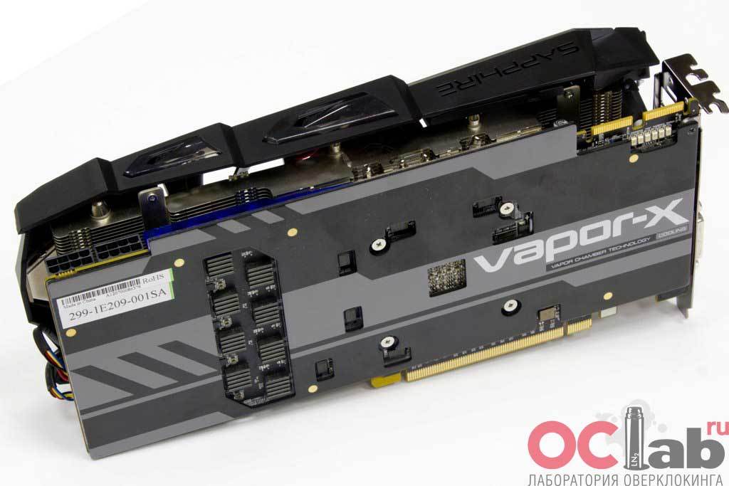
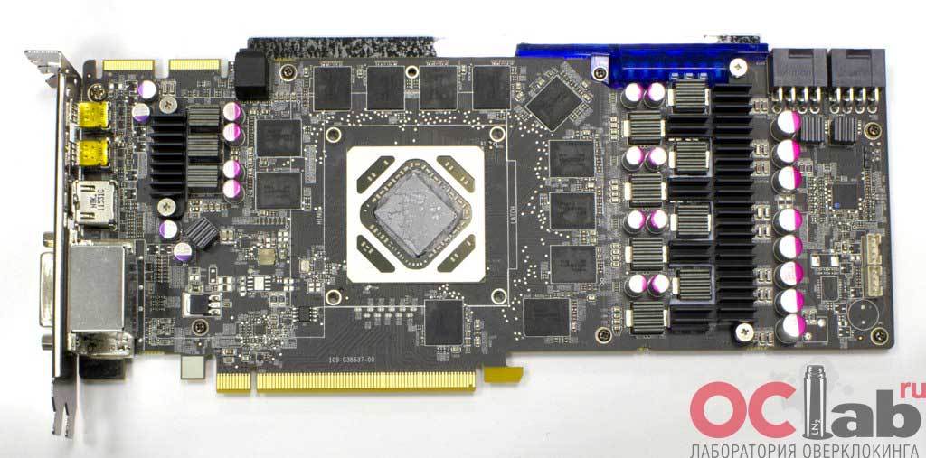
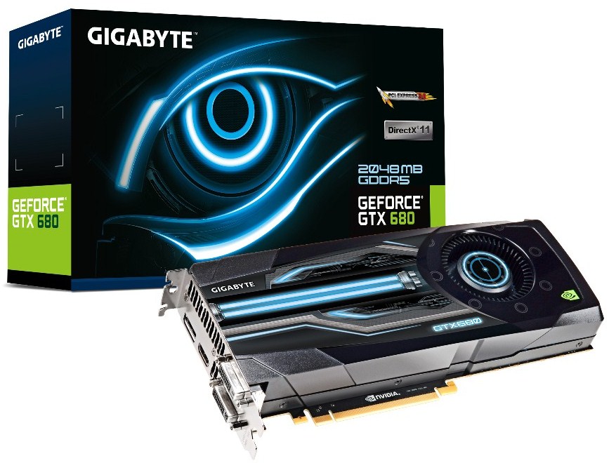
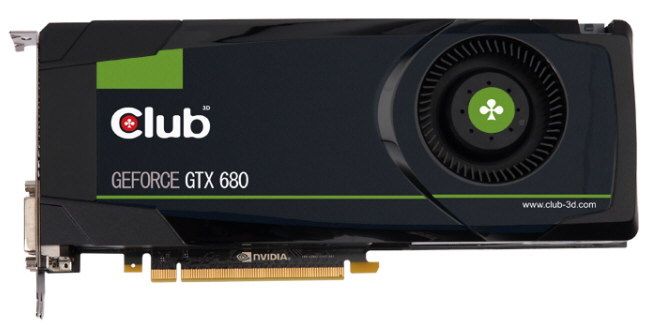
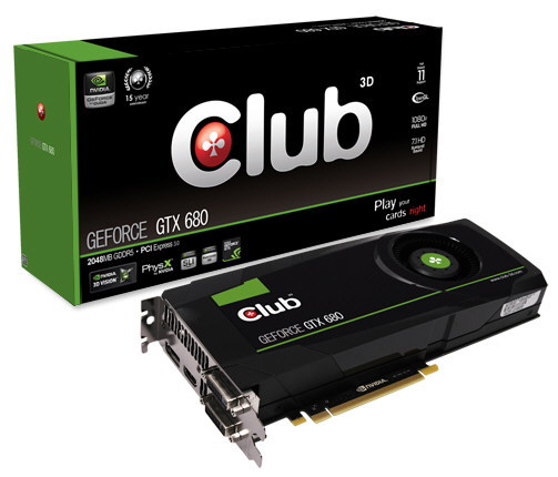
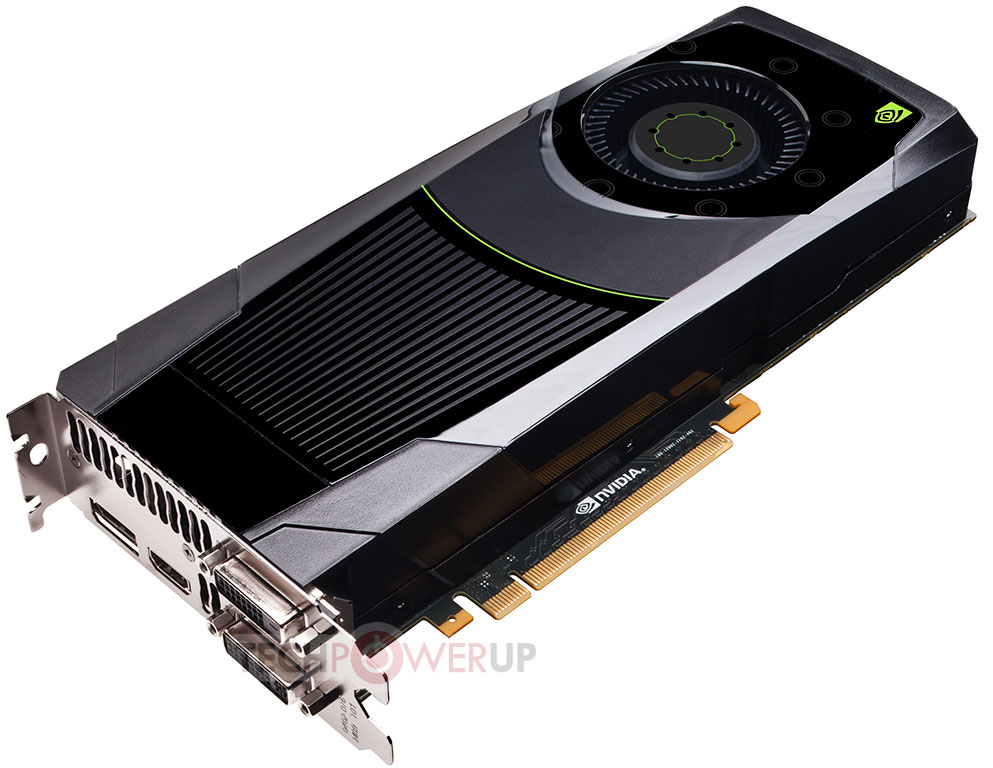
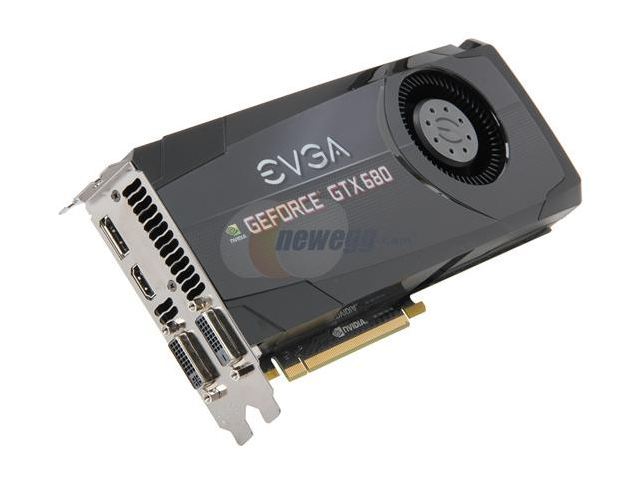
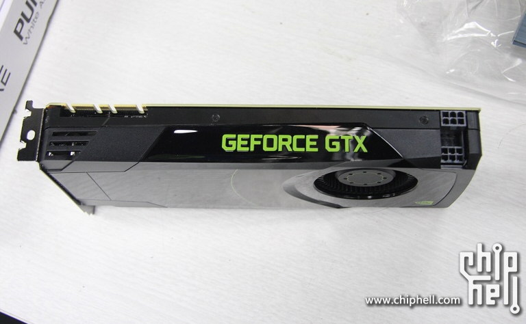
NVIDIA today launched the first model in the GeForce Kepler GPU family, the GeForce GTX 680. Based on the spanking new "Kepler" architecture, and a high-performance chip derived from it, GK104, and built on the 28 nm fab process at TSMC, the GeForce GTX 680 is NVIDIA's fresh bid for single-GPU performance supremacy. The new chip packs a staggering 1536 CUDA cores (three-fold increase over GTX 580), 2 GB of GDDR5 memory over a 256-bit wide memory interface, and staggering clock speeds of 1006 MHz (core base), 1056 MHz (core boost), and 1502 MHz (memory, 6.00 GHz effective), with a memory interface bandwidth of 192 GB/s.

It doesn't stop there. NVIDIA introduced a clever new technology called GPU Boost, which makes the GPU self-aware of parameters such as load, voltages, temperatures, and auto-tunes clock speeds, to deliver the best performance per Watt ratio. NVIDIA also introduced Adaptive V-Sync, which smooths transition between lower than refresh-rate frame-rates, and V-sync rate, attempting to eliminate lag, and naturally prevent page-tearing. NVIDIA also introduced the new TXAA anti-aliasing algorithm, which is a performance-efficient image quality enhancement. To top it all off, the chip has a TDP of just 195W. Available today, though leading retailers in mature markets, the NVIDIA GeForce GTX 680 is priced at US $499 (MSRP).

EVGA GeForce GTX 680 Pictured, Too, $499 Pricing Confirmed

Here is the first picture of EVGA GeForce GTX 680. The best-selling GeForce AIC partner in the US, EVGA, opted for a minimalist sticker design, while sticking to NVIDIA reference board and cooler designs. In fact, all GeForce GTX 680 launched in the first-wave, do. Speaking of first-wave, TechnoReviews managed to screengrab American Retailer Newegg.com listing out nearly all the GeForce GTX 680 models that will be available on launch of the SKU.

The listing confirms the US $499 (before taxes) pricing of NVIDIA GeForce GTX 680, because that's how low these cards are available for; they will never price it below NVIDIA-recommended MSRP. Newegg.com applying a $10 margin is quite natural, they've done it with pretty much every major graphics card market-launch this year, including that of the Radeon HD 7900 series. Assuming the GeForce GTX 680 beats Radeon HD 7970, as NVIDIA claims, our educated guess is it still won't start a "price-war" as such. AMD might recalibrate prices of HD 7900 series down 5~10%, but AMD and NVIDIA won't be able to drive prices below a threshold, and that threshold is governed by TSMC, its ability to ship 28 nm chips in volumes big enough, and at prices low enough, to support a price-war between the two GPU giants.

GK110 Specifications Approximated

Even as launch of the GK104-based GeForce GTX 680 nears, it's clear that it is emerging that it is not the fastest graphics processor in the GeForce Kepler family, if you sift through the specifications of the GK110 (yes, 110, not 100). Apparently, since GK104 meets or even exceeds the performance expectations of NVIDIA, the large-monolithic chip planned for this series, is likely codenamed GK110, and it's possible that it could get a GeForce GTX 700 series label.

3DCenter.org approximated the die size of the GK110 to be around 550 mm², 87% larger than that of the GK104. Since the chip is based on the 28 nm fab process, this also translates to a large increment in transistor count, up to 6 billion. The shader compute power is up by just around 30%, because the CUDA core count isn't a large increment (2000~2500 cores). The SMX (streaming multiprocessor 10) design could also face some changes. NVIDIA could prioritize beefing up other components than the CUDA cores, which could result in things such as a 512-bit wide GDDR5 memory interface. The maximum power consumption is estimated to be around 250~300 Watts. Its launch cannot be expected before August, 2012.

MSI Slips Out Some GeForce GTX 680 Marketing Material

NVIDIA's GeForce GTX 680 is certainly generating a lot of excitement, so much so that one AIB maker, MSI, has jumped the gun and put out a few PR goodies relating to the incoming card. Seen below, MSI's marketing materials show off the company's GTX 680 (which is based on NVIDIA's reference design), the new GEFORCE GTX logo, and some specs and features like the 2 GB of GDDR5 VRAM, the 256-bit memory interface, the quad display outputs, the PCI-Express 3.0 support, and the ability to run four monitors (and a complete 3D Vision Surround setup) from a single card.

MSI's GeForce GTX 680 will also be fully supported by the company's Afterburner utility that's set to provide 'GPU/Memory Clock Offset and Power Limit Control'. Expect an official unveiling of the MSI GeForce GTX 680 this Thursday, March 22nd.

- pictures removed at MSI's request -

AMD Radeon HD 7990 Clock Speeds, Chip-Configuration Surface

Closely trailing the launch of NVIDIA's GeForce GTX 680, and keeping up with its own streak of launching a new graphics card line each month since January, AMD will unveil its Radeon HD 7990 graphics card in April, or so it's reported. INPAI reports the clock-speed and chip-configuration of the upcoming dual-GPU monstrosity. The Radeon HD 7990 packs two 28 nm "Tahiti" GPUs as a "Crossfire on a stick" solution. The Tahiti chips will be clocked at 850 MHz (core), and 1250 MHz (5.00 GHz effective) memory.

The chip-configuration of each of the two Tahiti chips will be the same as that on the Radeon HD 7970, with 2048 Graphics CoreNext stream processors, 128 TMUs, 32 ROPs, and 384-bit wide GDDR5 memory interface, holding 3 GB of memory, each. The total memory on the card will hence be 6 GB. With the Radeon HD 7970 refusing to budge from its US $549 price-point, it's quite natural that the Radeon HD 7990 will be priced very high. It is gunning to retain the performance crown that's currently disputed between the Radeon HD 6990 and GeForce GTX 590.

TSMC Expanding 28 nm Manufacturing Facility

With the advent of highly-complex 28 nm discrete PC graphics processors, and ARM designers lined up with their increasingly powerful SoCs, TSMC is bound to see a pile up of orders for chips built on its newest bulk manufacturing process. In view of this, the "messiah of the fabless" is planning an expansion of its 28 nm manufacturing facility. This expansion is set to occur a little later in 2012. TSMC reportedly is running at full capacity at its 12-inch fabs because of strong demand for 28 nm as well as 40 nm and 65 nm. Due to this, some designers are approaching TSMC's competitors UMC and Samsung for 28 nm bulk manufacturing, according to sources. The expansion will follow a revision of TSMC's capex target for 2012, up from US $6 billion.

MSI Announces Next Generation R7970 Lightning Graphics Card

Leading international graphics card and mainboard maker MSI today announced the release of the MSI R7970 Lightning, the new heir to the throne of Lightning graphics cards. Equipped with AMD's 28 nm Radeon HD 7970 GPU, the MSI R7970 Lightning features an all-new Unlocked Digital Power Architecture that incorporates an Unlocked BIOS, Digital PWM Controller, and Enhanced Power Design to boost overclocking potential to new heights and make overclocking easier than ever.

In an industry first, the proprietary "GPU Reactor" power supply module reduces power supply noise and also boosts overclocking stability as well. To keep this beast cool, the MSI R7970 Lightning utilizes the latest Twin Frozr IV Thermal Design equipped with Dust Removal Technology. The dual 10 cm fans with Propeller Blade Technology generate massive airflow for fast heat dissipation while remaining whisper silent. The two form-in-one heat sinks improve cooling for memory and the power supply module as well ensure structural integrity.

Powercolor Adds a Flavor Into HD7700 Series: PCS+ HD7770 GHz Edition

TUL Corporation, a leading manufacturer of AMD graphic cards, today announces a new flavor into HD7700 series: the PCS+ HD7770 GHz Edition. Packed with factory overclocked setting, the PCS+ HD7770 delivers the out-of-box gaming performance with core speed at 1150 MHz and memory speed at 5.0 Gbps; based on the advanced 28 nm GCN architecture and PCI Express 3.0, the PCS+ HD7770 enables the best efficiency and extraordinary performance by doubling the bandwidth between GPU and CPU.

PowerColor PCS+ HD7770 has equipped with solid cooling design; by utilizing heat pipe direct touch technology, it can be cooled down efficiently through heat pipe which fully covers GPU, easily carrying away excessive heat from large extrusion heat sink and cooling fan on top. Moreover, with smart fan control technology, this edition enables the best user experience through automatically fan speed controlled.

New Acer Aspire Timeline M3 Packs GeForce GT 640M, Too

NVIDIA seems to have scored big design wins with Acer, for its next-generation GPUs. First, we had reports of Acer's VA40 combining Intel "Ivy Bridge" Core processors with NVIDIA GeForce GT 640M, and now Acer Timeline M3-581TG, following the same path. The M3-581TG is a 15.6-inch Ultrabook (one of the first of its kind). Pictures of this model reveal case-badges of its key components, including an NVIDIA GEFORCE GT case-badge, which gives out GPU model (GeForce GT 640M) and memory amount (1 GB). This could very well be the way NVIDIA's GeForce GT family of GPUs will be designated in case-badges.

Based on the 28 nm GK107 silicon, the GeForce GT 640M packs 384 CUDA cores running at speeds of up to 625 MHz, with 405 MHz base clock, and 910 MHz DDR3 memory, churning up 28.8 GB/s memory bandwidth. Other notable components of the Timeline M3-581TG include Intel Core i7-2637M (1.7 GHz dual-core, 4 MB of L3 cache) processor, 4 GB DDR3-1333 memory, and 256 GB SSD.

Next-Gen. Razer Blade Combines Ivy Bridge and Kepler

Even as the Razer's first gaming notebook, the Blade, has the guts to command a US $2,800 price for its dual-core processor and GeForce GT 555M graphics, which still went on to sell-out, according to its makers, its successor is already taking shape, suggests a BSN report. The next-generation Blade notebook is said to combine an Intel Core processor based on the 22 nm "Ivy Bridge" architecture, with NVIDIA's exciting new 28 nm graphics based on the Kepler architecture. The Razer Blade is what its makers claim to be "the world's first true gaming laptop."

New NVIDIA GeForce GTX 680 Pictures Hit The Web

Courtesy of ChipHell we now have a couple of fresh pictures of NVIDIA's first Kepler-powered graphics card, the GeForce (or should we write' GeFORCE') GTX 680. Shot both from above and the back, the incoming card has a black PCB, a dual-slot/single-fan cooler, two (stacked) 6-pin PCIe power plugs, a couple of SLI connectors, and four display outputs - dual DVI, HDMI and DisplayPort.

The GTX 680 is equipped with one GK104 28 nm GPU, and reportedly boasts 1536 CUDA Cores, a 256-bit memory interface, 2 GB of GDDR5 VRAM (4 GB models should also be in the works), PCI-Express 3.0, and a TDP of around 190 W. The GeForce GTX 680 is expected to be launched next week, on March 22nd. Its rumored price tag is $549.
Return to Keyword Browsing
May 15th, 2024 18:55 EDT change timezone

New Forum Posts

Popular Reviews

Controversial News Posts