News Posts matching #Foundry

Return to Keyword Browsing

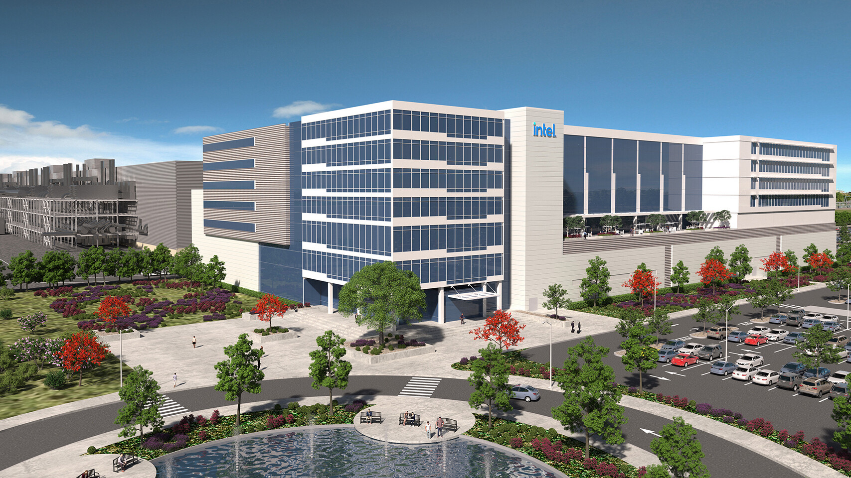
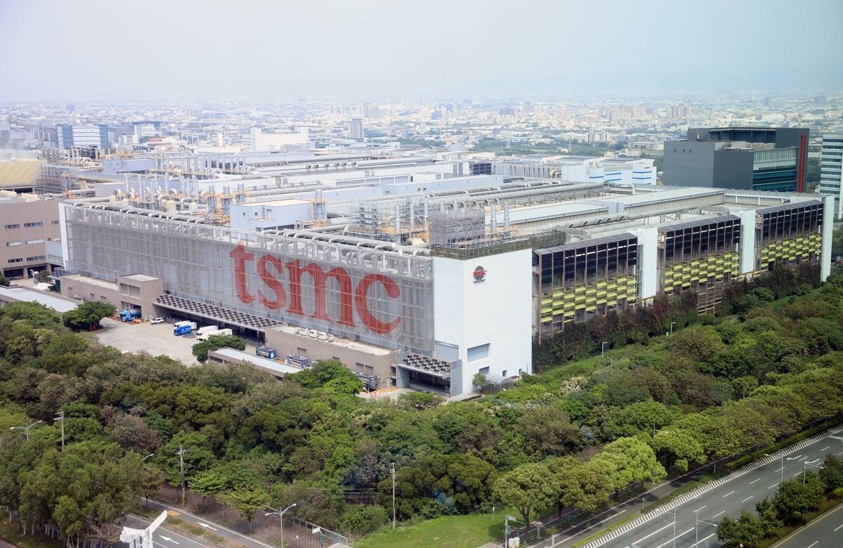
Intel Expects to Beat TSMC at 2nm, Intel Foundry to Operate Almost as a Separate Business

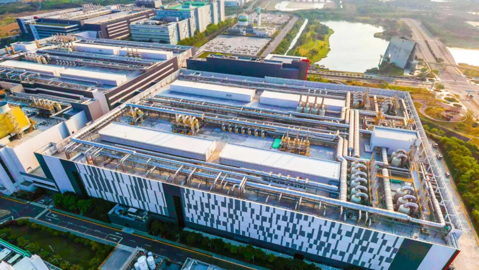
Intel's integrated device manufacturing (IDM) has been experiencing a lot of trouble in recent years, and the company is not a leading-edge semiconductor manufacturer, with TSMC taking the pole position. However, the new restructuring hopes to change some of the business operations to increase its efficiency and establish Intel as the go-to foundry for customers. David Zinsner, Executive Vice President and the Chief Financial Officer, alongside Jason Grebe, Corporate Vice President & GM of the Corporate Planning Group at Intel, joined investors to explain how IDM will transform into a next-generation business. Intel IDM, including Intel Foundry Services (IFS), will get a new operation model, which will put IDM as an almost separate business unit with its own profit and loss (P&L) statement published in the quarterly/yearly financial report.

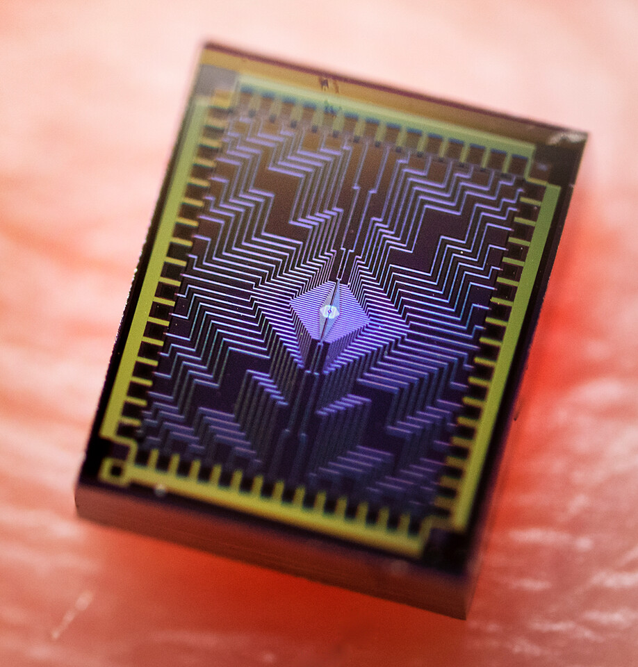
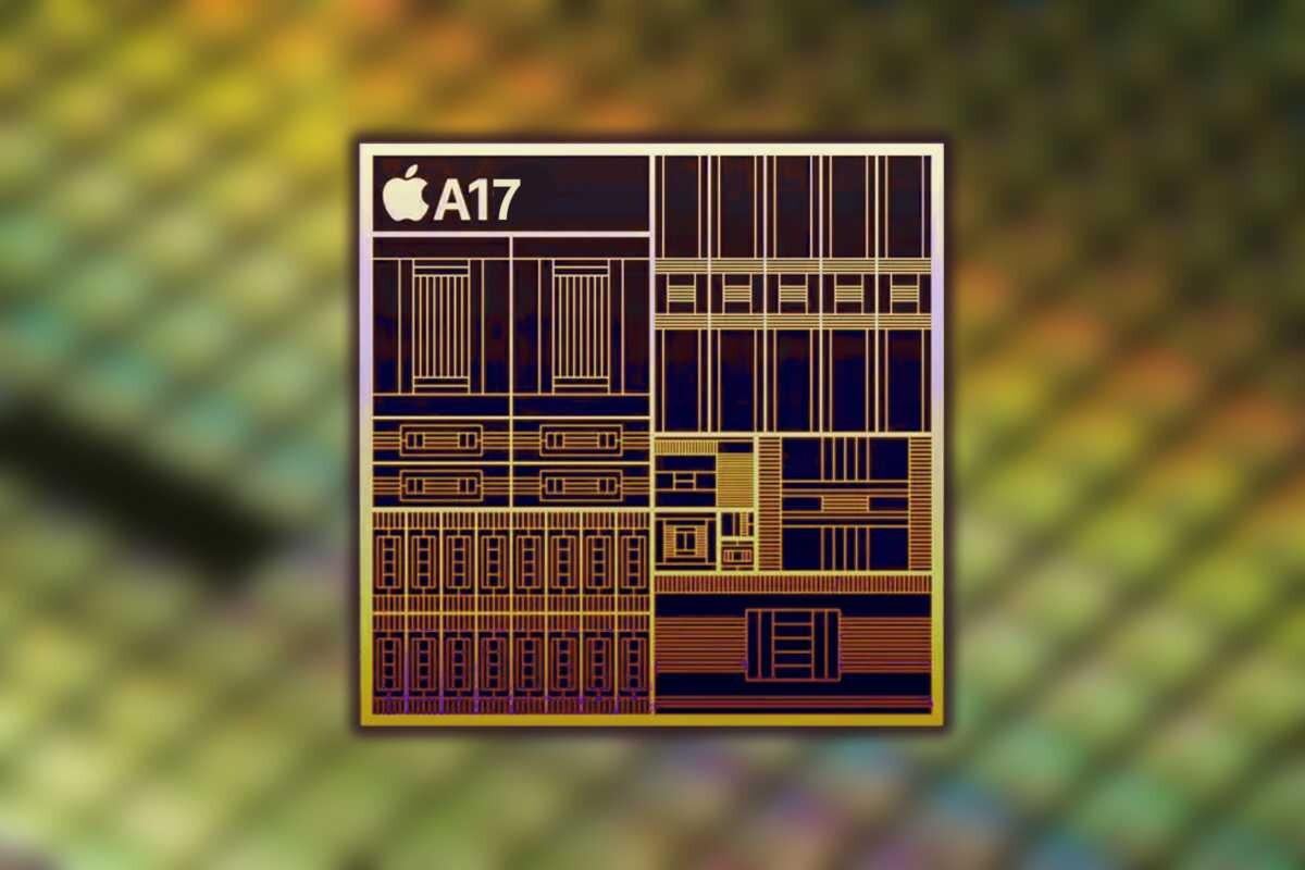
According to Intel, the company's IDM 1.0 strategy has been serving it well, but IDM 2.0 is needed to build next-generation nodes as the capital required for them is massive. Intel hopes to regain node leadership with the Intel 18A node in 2025. The company's strategy is still to have IFS as the second biggest external foundry business, presumably just behind TSMC. Putting IDM into its own P&L will result in $8-10 billion in "cost reduction opportunities, " including ramp rates, test time, and sort times based on the market pricing, not Intel's pricing. At the start, IDM is expected o start with a negative operating margin. Intel also states that keeping IFS as a business unit allows the company to simultaneously develop products on it and de-risk it for customers who want to build on IFS. The company is developing five different products (assuming packaging) on Intel 18A, all of which will be available for customers to use as well.

Intel, German Government Agree on Increased Scope for Wafer Fabrication Site in Magdeburg

Intel and the German federal government have signed a revised letter of intent for Intel's planned leading-edge wafer fabrication site in Magdeburg, the capital of Saxony-Anhalt state in Germany. The agreement encompasses Intel's expanded investment in the site, now expected to be more than 30 billion euros for two first-of-a-kind semiconductor facilities (also known as "fabs") in Europe, along with increased government support that includes incentives, reflecting the expanded scope and change in economic conditions since the site was first announced.

Intel acquired the land for the project in November 2022, and the first facility is expected to enter production in four to five years following the European Commission's approval of the incentive package. Given the current timeline and scale of the investment, Intel plans to deploy more advanced Angstrom-era technology in the facilities than originally envisioned. The Magdeburg site will serve Intel products and Intel Foundry Services customers.

Intel's New Chip to Advance Silicon Spin Qubit Research for Quantum Computing

Today, Intel announced the release of its newest quantum research chip, Tunnel Falls, a 12-qubit silicon chip, and it is making the chip available to the quantum research community. In addition, Intel is collaborating with the Laboratory for Physical Sciences (LPS) at the University of Maryland, College Park's Qubit Collaboratory (LQC), a national-level Quantum Information Sciences (QIS) Research Center, to advance quantum computing research.

"Tunnel Falls is Intel's most advanced silicon spin qubit chip to date and draws upon the company's decades of transistor design and manufacturing expertise. The release of the new chip is the next step in Intel's long-term strategy to build a full-stack commercial quantum computing system. While there are still fundamental questions and challenges that must be solved along the path to a fault-tolerant quantum computer, the academic community can now explore this technology and accelerate research development."—Jim Clarke, director of Quantum Hardware, Intel

Synopsys and Samsung Collaborate to Deliver Broad IP Portfolio Across All Advanced Samsung Foundry Processes

Synopsys, Inc. today announced an expanded agreement with Samsung Foundry to develop a broad portfolio of IP to reduce design risk and accelerate silicon success for automotive, mobile, high-performance computing (HPC) and multi-die designs. This agreement expands Synopsys' collaboration with Samsung to enhance the Synopsys IP offering for Samsung's advanced 8LPU, SF5, SF4 and SF3 processes and includes Foundation IP, USB, PCI Express, 112G Ethernet, UCIe, LPDDR, DDR, MIPI and more. In addition, Synopsys will optimize IP for Samsung's SF5A and SF4A automotive process nodes to meet stringent Grade 1 or Grade 2 temperature and AEC-Q100 reliability requirements, enabling automotive chip designers to reduce their design effort and accelerate AEC-Q100 qualification. The auto-grade IP for ADAS SoCs will include design failure mode and effect analysis (DFMEA) reports that can save months of development effort for automotive SoC applications.

"Our extensive co-optimization efforts with Samsung across both EDA and IP help automotive, mobile, HPC, and multi-die system architects cope with the inherent challenges of designing chips for advanced process technologies," said John Koeter, senior vice president of product management and strategy for IP at Synopsys. "This extension of our decades-long collaboration provides designers with a low-risk path to achieving their design requirements and quickly launching differentiated products to the market."

RIKEN and Intel Collaborate on "Road to Exascale"

RIKEN and Intel Corporation (hereafter referred to as Intel) have signed a memorandum of understanding on collaboration and cooperation to accelerate joint research in next-generation computing fields such as AI (artificial intelligence), high-performance computing, and quantum computers. The signing ceremony was concluded on May 18, 2023. As part of this MOU, RIKEN will work with Intel Foundry Services (IFS) to prototype these new solutions.

Intel to Demonstrate PowerVia on E-Core Processor Built with Intel 4 Node

At VLSI Symposium 2023, scheduled to take place between June 11-16, Intel is set to demonstrate its PowerVia technology working efficiently on an E-Core chip built using the Intel 4 node. Conventional chips have power and signal interconnects distributed across multiple metal layers. PowerVia, on the other hand, dedicates specific layers for power delivery, effectively separating them from the signal routing layers. This approach allows for vertical power delivery through a set of power-specific Through-Silicon Vias (TSVs) or PowerVias, which are essentially vertical connections between the top and bottom surfaces of the chip. By delivering power directly from the backside of the chip, PowerVia reduces power supply noise and resistive losses, optimizing power distribution and improving overall energy efficiency. PowerVia is set to make a debut in 2024 with Intel 20A node.

For VLSI Symposium 2023 talk, the company has prepared a paper that highlights a design made using Intel 4 technology and implements E-Cores only in a test chip. The document states: "PowerVia Technology is a novel innovation to extend Process Scaling by having Power Delivery on the backside. This paper presents the pre and post silicon findings from implementing an Intel E-Core in PowerVia Technology. PowerVia enabled standard cell utilization of greater than 90 percent in large areas of the core while showing greater than 5 percent frequency benefit in silicon due reduced IR drop. Successful Post silicon debug is demonstrated with slightly higher but acceptable throughput times. The thermal characteristics of the PowerVia testchip is inline with higher power densities expected from logic scaling."

Fire at TSMC Arizona Plant a Minor Episode, North Taiwan Facility Damaged in Separate Incident

TSMC has confirmed to Taiwan News this weekend that a fire at its Phoenix-general area, Arizona semiconductor plant was only "limited to an outside trash chute and immediately extinguished" - the chipmaker was responding to an afternoon incident from Friday (April 28). A worker took photos of black smoke rising from a section of the brand new factory, the employee then proceeded to share their snaps online via a discussion board. A local firefighting crew extinguished the blaze soon after evacuating workers from the affected area, a preliminary investigation conducted by the emergency responders found that the fire originated from a waste/refuse chute. A root cause has not yet been identified according to the newspaper's article.

The Arizona plant was not the only TSMC location to play host to an unexpected incident this week - reports from Wednesday (April 26) state that a fire broke out during the (preceding) evening/night at a company facility in North Taiwan. No injuries or casualties were reported following a response by firefighters who had the situation under control soon after 9 pm - TSMC believes that the fire started at around 19:30. The incomplete factory is situated within Taiwan's Hsinchu Science Park, and is set to bolster the company's existing advanced 3D IC package manufacturing efforts. Part of the facility will also be setup as a component testing lab. TSMC has declared that it is conducting an investigation into the incident at its Zhunan, Miaoli County location.

Samsung Electronics Announces First Quarter 2023 Results, Profits Lowest in 14 Years

Samsung Electronics today reported financial results for the first quarter ended March 31, 2023. The Company posted KRW 63.75 trillion in consolidated revenue, a 10% decline from the previous quarter, as overall consumer spending slowed amid the uncertain global macroeconomic environment. Operating profit was KRW 0.64 trillion as the DS (Device Solutions) Division faced decreased demand, while profit in the DX (Device eXperience) Division increased.

The DS Division's profit declined from the previous quarter due to weak demand in the Memory Business, a decline in utilization rates in the Foundry Business and continued weak demand and inventory adjustments from customers. Samsung Display Corporation (SDC) saw earnings in the mobile panel business decline quarter-on-quarter amid a market contraction, while the large panel business slightly narrowed its losses. The DX Division's results improved on the back of strong sales of the premium Galaxy S23 series as well as an enhanced sales mix focusing on premium TVs.

Intel Foundry and Arm Announce Multigeneration Collaboration on Leading-Edge SoC Design

Intel Foundry Services (IFS) and Arm today announced a multigeneration agreement to enable chip designers to build low-power compute system-on-chips (SoCs) on the Intel 18A process. The collaboration will focus on mobile SoC designs first, but allow for potential design expansion into automotive, Internet of Things (IoT), data center, aerospace and government applications. Arm customers designing their next-generation mobile SoCs will benefit from leading-edge Intel 18A process technology, which delivers new breakthrough transistor technologies for improved power and performance, and from IFS's robust manufacturing footprint that includes U.S.- and EU-based capacity.

"There is growing demand for computing power driven by the digitization of everything, but until now fabless customers have had limited options for designing around the most advanced mobile technology," said Pat Gelsinger, CEO of Intel Corporation. "Intel's collaboration with Arm will expand the market opportunity for IFS and open up new options and approaches for any fabless company that wants to access best-in-class CPU IP and the power of an open system foundry with leading-edge process technology."

Apple A17 Bionic SoC Performance Targets Could be Lowered

Apple's engineering team is rumored to be adjusting performance targets set for its next generation mobile SoC - the A17 Bionic - due to issues at the TSMC foundry. The cutting edge 3 nm process is proving difficult to handle, according to industry tipsters on Twitter. The leaks point to the A17 Bionic's overall performance goals being lowered by 20%, mainly due to the TSMC N3B node not meeting production targets. The factory is apparently lowering its yield and execution targets due to ongoing problems with FinFET limitations.

The leakers have recently revealed more up-to-date A17 Bionic's Geekbench 6 scores, with single thread performance at 3019, and multi-thread at 7860. Various publications have been hyping the mobile SoC's single thread performance as matching that of desktop CPUs from Intel and AMD, more specifically 13th-gen Core i7 and 'high-end' Ryzen models. Naturally the A17 Bionic cannot compete with these CPUs in terms of multi-thread performance.

Global Fab Equipment Spending on Track for 2024 Recovery After 2023 Slowdown

Global fab equipment spending for front-end facilities is expected to decrease 22% year-over-year (YoY) to US$76 billion in 2023 from a record high of US$98 billion in 2022 before rising 21% YoY to US$92 billion in 2024 to reclaim lost ground, SEMI announced today in its latest quarterly World Fab Forecast report. The 2023 decline will stem from weakening chip demand and higher inventory of consumer and mobile devices.

Next year's fab equipment spending recovery will be driven in part by the end of the semiconductor inventory correction in 2023 and strengthening demand for semiconductors in the high-performance computing (HPC) and automotive segments. "This quarter's SEMI World Fab Forecast update offers our first look ahead to 2024, highlighting the steady global expansion of fab capacity to support future semiconductor industry growth driven by the automotive and computing segments and a host of emerging applications," said Ajit Manocha, SEMI president and CEO. "The report points to a healthy 21% uptick in equipment investment next year."

Samsung Hires ex TSMC Executive to Improve Advanced IC Packaging

Business Korea got the scoop on Samsung hiring an ex TSMC executive by the name of Lin Jun-Cheng, who was with TSMC for almost 19 years. His role at Samsung will be as VP of Samsung's advanced packaging business, something he should be more than familiar with, as during his time at TSMC, he was part of no less than 450 patents involving chip packaging. Lin has also worked for Micron and more recently for a company called Skytech, that specialises in advanced IC packaging equipment.

Samsung has relied on third parties when it comes to more advanced chip packaging and has been behind Intel and TSMC in this area. The Business Korea article mentions that Samsung has been spending a lot of resources over the past year to build its own advanced packaging business, including hiring industry experts. Samsung has hired ex Apple, Intel and Qualcomm staff to join or head various teams related to its foundry division, not only for packaging, but also experts in various lithography processes, such as EUV. Samsung is clearly taking its foundry business seriously, even though they have had their fair share of issues with various customers over the past few years.

Price War Looming for Mature Fab Nodes in Taiwan

The smaller foundries in Taiwan—at least compared to TSMC—UMC, PSMC and VIS to name the bigger players, but also other less well known foundries that produce chips on mature nodes, are getting ready for what looks like a price war. In all fairness, all of these companies have hiked their prices multiple times over the past couple of years, so it might just be a return to more normal pricing for these nodes that we're looking at. According to UDN media in Taiwan, the smaller foundries are offering discounts that range between 10 and 20 percent for new orders placed with them.

This is largely due to underutilised production lines for some nodes and the companies are trying to increase the utilisation rate of these nodes. The article mentions that the foundries with 8-inch wafer lines are those hardest hit, especially as they've produced more specialised ICs, such as fingerprint sensors, various driver ICs and power management ICs to mention a few. Some of these foundries are now running at 50 to 60 percent of their capacity, which doesn't bode well for the industry. On the other hand, 12-inch fabs aren't nearly as badly hit and might not offer as attractive discounts to potential customers. Another threat to the Taiwanese foundries is Samsung, which is reportedly also offering around a 10 percent discount on its mature nodes.

Intel Foundry Services Allegedly Working on Test Chips for 43 Potential Customers

A new story is making the rounds, citing Wang Rui, chair Intel China, in the media in both China and Taiwan, claiming that Intel is working on test chips for as many as 43 potential customers for Intel Foundry Services (IFS). At least seven of those potential customers are said to be from the top 10 foundry clients globally. This sounds a bit too good to be true, considering that IFS has as yet to prove that they can deliver on their promises.

Furthermore, Wang Rui is meant to have gone on record, saying that IFS has taped out products on both its 20A and 18A nodes. Exactly what these products are, wasn't divulged, but as the 18A node isn't expected to go into mass production until the second half of 2024, this sounds a little bit too good to be true. What makes this even less believable is that the Intel 4 node is only set to go into mass production in the second half this year and before Intel moves to its Ångström nodes, the company still has to deliver on its Intel 3 node. The Intel China chair is also reportedly confident that Intel will be returning to a leading foundry position by 2025.

Samsung Electronics Announces Fourth Quarter and FY 2022 Results, Profits at an 8-year Low

Samsung Electronics today reported financial results for the fourth quarter and the fiscal year 2022. The Company posted KRW 70.46 trillion in consolidated revenue and KRW 4.31 trillion in operating profit in the quarter ended December 31, 2022. For the full year, it reported 302.23 trillion in annual revenue, a record high and KRW 43.38 trillion in operating profit.

The business environment deteriorated significantly in the fourth quarter due to weak demand amid a global economic slowdown. Earnings at the Memory Business decreased sharply as prices fell and customers continued to adjust inventory. The System LSI Business also saw a decline in earnings as sales of key products were weighed down by inventory adjustments in the industry. The Foundry Business posted a new record for quarterly revenue while profit increased year-on-year on the back of advanced node capacity expansion as well as customer base and application area diversification.

Foundry Revenue is Forecasted to Drop by 4% YoY for 2023, TrendForce Notes

TrendForce's recent analysis of the foundry market reveals that demand continues to slide for all types of mature and advanced nodes. The major IC design houses have cut wafer input for 1Q23 and will likely scale back further for 2Q23. Currently, foundries are expected to maintain a lower-than-ideal level of capacity utilization rate in the first two quarters of this year. Some nodes could experience a steeper demand drop in 2Q23 as there are still no signs of a significant rebound in wafer orders. Looking ahead to the second half of this year, orders will likely pick up for some components that underwent an inventory correction at an earlier time. However, the state of the global economy will remain the largest variable that affect demand, and the recovery of individual foundries' capacity utilization rates will not occur as quickly as expected. Taking these factors into account, TrendForce currently forecasts that global foundry revenue will drop by around 4% YoY for 2023. The projected decline for 2023 is more severe when compared with the one that was recorded for 2019.

Global Total Semiconductor Equipment Sales Forecast to Reach Record High in 2022

Global sales of total semiconductor manufacturing equipment by original equipment manufacturers are forecast to reach a new high of $108.5 billion in 2022, rising 5.9% from the previous industry record of $102.5 billion in 2021, SEMI announced today in its Year-End Total Semiconductor Equipment Forecast - OEM Perspective at SEMICON Japan 2022. The record high caps three consecutive years of record revenue. The global total semiconductor manufacturing equipment market is expected to contract to $91.2 billion next year before rebounding in 2024 driven by both the front-end and back-end segments.

"Record fab constructions have driven total semiconductor manufacturing equipment sales to cross the $100 billion mark for a second straight year," said Ajit Manocha, SEMI president and CEO. "Emerging applications in multiple markets have set expectations for significant semiconductor industry growth this decade, which will necessitate further investments to expand production capacity."

Global Top 10 Foundries' Total Revenue Grew by 6% QoQ for 3Q22, but Foundry Industry's Revenue Performance Will Enter Correction Period in 4Q22

According to TrendForce's research, the total revenue of the global top 10 foundries rose by 6% QoQ to US$35.21 billion for 3Q22 as the release of the new iPhone series during the second half of the year generated significant stock-up activities across Apple's supply chain. However, the global economy shows weak performances, and factors such as China's policy on containing COVID-19 outbreaks and high inflation continue to impact consumer confidence. As a result, peak-season demand in the second half of the year has been underwhelming, and inventory consumption is proceeding slower than anticipated. This situation has led to substantial downward corrections to foundry orders as well. For 4Q22, TrendForce forecasts that the total revenue of the global top 10 foundries will register a QoQ decline, thereby terminating the boom of the past two years—when there was an uninterrupted trend of QoQ revenue growth.

Regarding individual foundries' performances in 3Q22, the group of the top five was led by TSMC, followed by Samsung, UMC, GlobalFoundries, and SMIC. Their collective global market share (in revenue terms) came to 89.6%. Most foundries were directly impacted by clients slowing down their stock-up activities or significantly correcting down their orders. Only TSMC was able to make a notable gain due to Apple's strong stock-up demand for the SoCs deployed in this year's new iPhone models. TSMC saw its revenue rise by 11.1% QoQ to US$20.16 billion, and the corresponding market share expanded to 56.1%. The growth was mainly attributed to the ≤7 nm nodes, whose share in the foundry's revenue had kept climbing and reached 54% in the third quarter. Conversely, Samsung actually experienced a slight QoQ drop of 0.1% in foundry revenue even though it had also benefited from the component demand related to the new iPhone series. Partially impacted by the weakening of the Korean won, Samsung's market share fell to 15.5%.

One of TSMC's Biggest Customers Cuts 3nm Wafer Orders As Consumer Demand Deflates

A major unnamed customer of TSMC has reportedly cut their order for 3 nm wafers. Foundry customers usually place orders for cutting-edge foundry nodes several quarters in advance, in exchange for priority foundry allocations, and preferential rates, while foundries use revenues from these orders to develop the capacity for manufacture these chips. The 3 nm customer could be anyone—Qualcomm, Mediatek, NVIDIA, AMD, or Intel. Order cancellations have reportedly had a domino-effect on the upstream supply-chain of TSMC, hitting suppliers of raw materials, manufacturing equipment, and other consumables. There is an industry-wide slump in demand for consumer electronics and PC hardware, which reflects in the slump in revenues and/or guidance in quarterly financial results releases by prominent companies.

Global 300 mm Semiconductor Fab Capacity Projected To Reach New High in 2025

Semiconductor manufacturers worldwide are forecast to expand 300 mm fab capacity at a nearly 10% compound average growth rate (CAGR) from 2022 to 2025, reaching an all-time high of 9.2 million wafers per month (wpm), SEMI announced today in its 300 mm Fab Outlook to 2025 report. Strong demand for automotive semiconductors and new government funding and incentive programs in multiple regions are driving much of the growth.

"While shortages of some chips have eased and supply of others has remained tight, the semiconductor industry is laying the groundwork to meet longer-term demand for a broad range of emerging applications as it expands 300 mm fab capacity," said Ajit Manocha, SEMI President and CEO. "SEMI is currently tracking 67 new 300 mm fabs or major additions of new lines expected to start construction from 2022 to 2025."

Samsung Electronics Unveils Plans for 1.4 nm Process Technology

Samsung Electronics, a world leader in advanced semiconductor technology, announced today a strengthened business strategy for its Foundry Business with the introduction of cutting-edge technologies at its annual Samsung Foundry Forum event. With significant market growth in high-performance computing (HPC), artificial intelligence (AI), 5/6G connectivity and automotive applications, demand for advanced semiconductors has increased dramatically, making innovation in semiconductor process technology critical to the business success of foundry customers. To that end, Samsung highlighted its commitment to bringing its most advanced process technology, 1.4-nanometer (nm), for mass production in 2027.

During the event, Samsung also outlined steps its Foundry Business is taking in order to meet customers' needs, including: foundry process technology innovation, process technology optimization for each specific applications, stable production capabilities, and customized services for customers. "The technology development goal down to 1.4 nm and foundry platforms specialized for each application, together with stable supply through consistent investment are all part of Samsung's strategies to secure customers' trust and support their success," said Dr. Si-young Choi, president and head of Foundry Business at Samsung Electronics. "Realizing every customer's innovations with our partners has been at the core of our foundry service."

More Details Emerge on Mediatek's Intel Foundry Plans

Last week's news about Mediatek signing an agreement to use Intel's Foundry Services (IFS) led to some speculation as to what Mediatek would be manufacturing at IFS. Details have now emerged in the Taiwan press about Mediatek's plans and the first products will be using the Intel 16 process, what was previously known as its 22 nm node. As such, we're not talking about anything cutting edge or even remotely close, but that's hardly a problem for Mediatek, as the company makes a vast range of products suitable for the node.

MediaTek CEO Rick Tsai mentioned that IFS will be used for producing semiconductors for digital TVs and wireless access networks at an investor conference in Taiwan. This suggests that most of the components might not even be for Mediatek itself, but rather its subsidiaries, such as MStar or Airoha. MStar is a company that produces a wide range of lower-end smart TV chips, whereas Airoha has ended up taking over Mediatek's networking and Bluetooth business units. Admittedly, Mediatek still has some of these types of products under its own brand, but these tend to be higher-end products that would require a more advanced node than 22 nm in most cases. Mediatek's move to IFS has raised concerns in Taiwan that the smaller foundries might be losing business from Mediatek over time, which means that UMC and PSMC are going to be on the losing end of this deal.

Intel and MediaTek Form Foundry Partnership

Intel and MediaTek today announced a strategic partnership to manufacture chips using Intel Foundry Services' (IFS) advanced process technologies. The agreement is designed to help MediaTek build a more balanced, resilient supply chain through the addition of a new foundry partner with significant capacity in the United States and Europe. MediaTek plans to use Intel process technologies to manufacture multiple chips for a range of smart edge devices. IFS offers a broad manufacturing platform with technologies optimized for high performance, low power and always-on connectivity built on a roadmap that spans production-proven three-dimensional FinFET transistors to next-generation breakthroughs.

"As one of the world's leading fabless chip designers powering more than 2 billion devices a year, MediaTek is a terrific partner for IFS as we enter our next phase of growth," said IFS President Randhir Thakur. "We have the right combination of advanced process technology and geographically diverse capacity to help MediaTek deliver the next billion connected devices across a range of applications."

Microsoft Azure Joins Intel Foundry Services Cloud Alliance

The recent semiconductor shortage has put an unprecedented amount of focus on the industry. Both commercial and government entities have come to recognize the lack of advanced node semiconductor manufacturing capabilities onshore in the United States. Intel Foundry Services (IFS) entry into the commercial foundry space is poised to change all that. As part of IFS Accelerator program, Intel recently announced their new IFS Cloud Alliance program, with Microsoft Azure as one of the inaugural members.

This is the latest chapter in a partnership between Intel and Microsoft that stretches back decades all the way back to the early days of the personal computer. In the last few years, Intel and Microsoft have collaborated on advancing semiconductor design on the cloud by working together to bring out EDA centric cloud compute such as the FX series on Azure, working with EDA vendors to enhance their software to better take advantage of the elasticity of the Azure cloud, as well as collaborating on a secure cloud-based semiconductor development platform for the US Department of Defense RAMP and RAMP-C programs.

Samsung Adopts Ansys' Simulation Portfolio to Create Semiconductor Designs to Optimize High-Speed Connectivity

Samsung Foundry will engage Ansys' industry-leading electromagnetic (EM) simulation tools to develop ultramodern designs, including 5G/6G, on the most advanced chips, nodes, and process technologies. Ansys' simulation solutions will deliver a comprehensive EM-aware design flow with greater capacity, speed, and integration capabilities for Samsung's most advanced semiconductor technology, accelerating on-chip design cycle times to boost high-speed connectivity while helping to reduce design error and risk.

Samsung designers will leverage Ansys' EM design tools, Ansys RaptorX, Ansys VeloceRF, and Ansys Exalto, to help reduce time to market by two to three weeks on smaller designs and up to two months for complex designs. With automation capabilities that optimize calculations and modeling, coupled with larger capacity, Ansys' software will allow the Samsung team to design at faster speeds with higher fidelity.
Return to Keyword Browsing
May 15th, 2024 18:57 EDT change timezone

New Forum Posts

Popular Reviews

Controversial News Posts