News Posts matching #Foundry

Return to Keyword Browsing

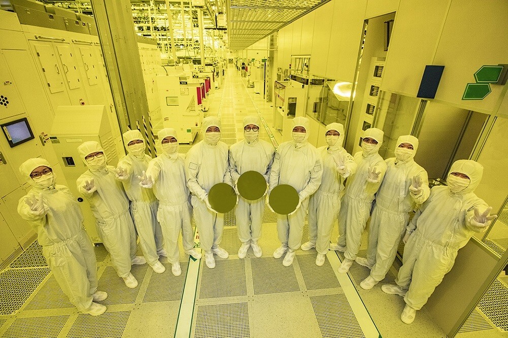
Samsung Begins Chip Production Using 3nm Process Technology With GAA Architecture

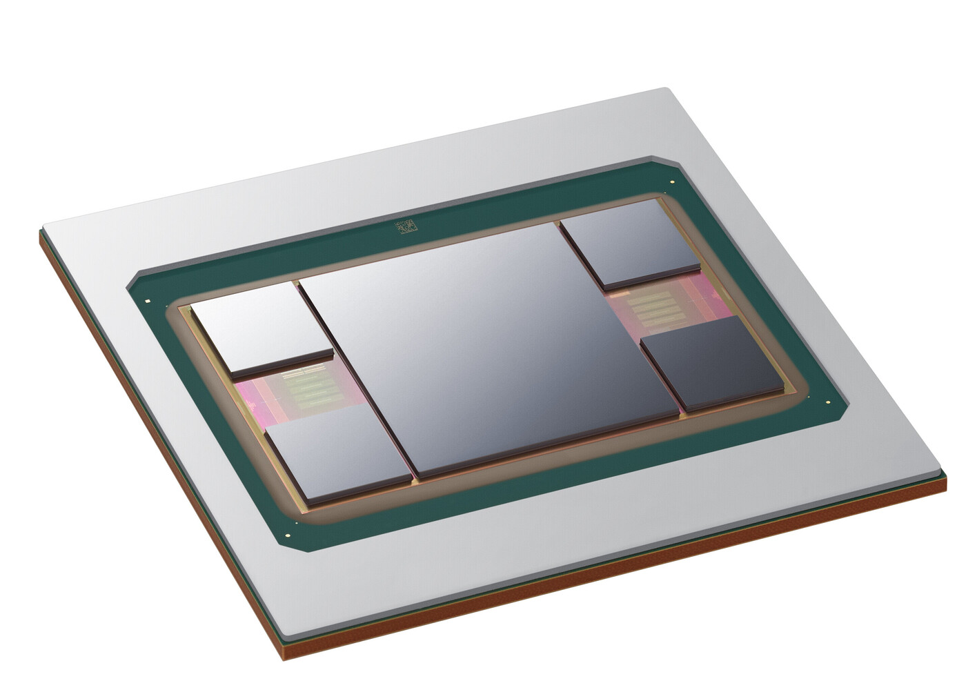
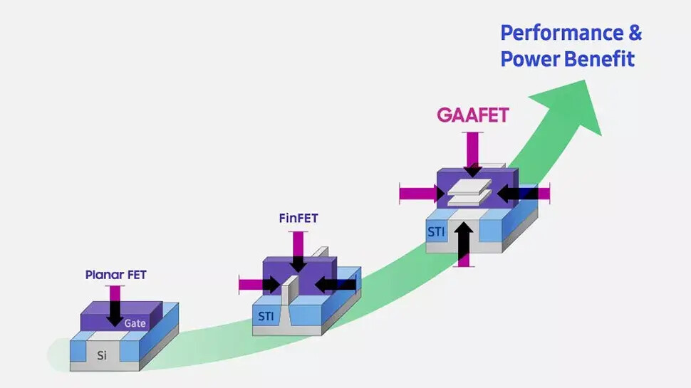
Samsung Electronics, the world leader in semiconductor technology, today announced that it has started initial production of its 3-nanometer (nm) process node applying Gate-All-Around (GAA) transistor architecture. Multi-Bridge-Channel FET (MBCFET), Samsung's GAA technology implemented for the first time ever, defies the performance limitations of FinFET, improving power efficiency by reducing the supply voltage level, while also enhancing performance by increasing drive current capability. Samsung is starting the first application of the nanosheet transistor with semiconductor chips for high performance, low power computing application and plans to expand to mobile processors.

"Samsung has grown rapidly as we continue to demonstrate leadership in applying next-generation technologies to manufacturing, such as foundry industry's first High-K Metal Gate, FinFET, as well as EUV. We seek to continue this leadership with the world's first 3 nm process with the MBCFET," said Dr. Siyoung Choi, President and Head of Foundry Business at Samsung Electronics. "We will continue active innovation in competitive technology development and build processes that help expedite achieving maturity of technology."

Off-season Offsets Wafer Pricing Increase, 1Q22 Foundry Output Value Up 8.2% QoQ, Says TrendForce

According to TrendForce research, although demand for consumer electronics remains weak, structural growth demand in the semiconductor industry including for servers, high-performance computing, automotive, and industrial equipment has not flagged, becoming a key driver for medium and long term foundry growth. At the same time, due to robust wafer production at higher pricing in 1Q22, quarterly output value hit a new high for the 11th consecutive quarter, reaching US$31.96 billion, 8.2% QoQ, marginally less than the previous quarter. In terms of ranking, the biggest change is Nexchip surpassed Tower at the ninth position.

TSMC's across the board wafer hikes in 4Q21 on batches primarily produced in 1Q22 coupled with sustained strong demand for high-performance computing and better foreign currency exchange rates pushed TSMC's 1Q22 revenue to $17.53 billion, up 11.3% QoQ. Quarterly revenue growth by node was generally around 10% and the 7/6 nm and 16/12 nm processes posted the highest growth rate due to small expansions in production. The only instance of revenue decline came at the 5/4 nm process due to Apple's iPhone 13 entering the off season for production stocking.

TSMC Said to be Eyeing Singapore for Fab Expansion

The rumour mill never seems to stop churning when it comes to TSMC and now the company is said to be looking at the tiny nation of Singapore for a future fab. This time the information comes via the Wall Street Journal rather than the usual Taiwanese sources and although the publication points out that no decision has been made at this point in time, it says that TSMC is apparently in talks with the Economic Development Board of Singapore. The official statement from the TSMC on the matter is that the company "doesn't rule out any possibility but does not have any concrete plan at this time".

The potential Singapore Fab would be producing 28 to 7 nm chips, in other words, quite far from TSMC's cutting edge nodes. However, TSMC is already building a similar facility in the southern city of Kaohsiung in Taiwan that's scheduled for opening in 2024. As such, the nodes used in a future facility in Singapore might change depending on when the fab will open and it might end up producing chips on more advanced nodes as well. As these fabs take a few years to get going, they're not projects that are started on a whim. We should also mention that TSMC already has a joint venture in Singapore together with NXP, called SSMC, which also produces for third parties.

Samsung Foundry Considering up to 20 Percent Price Hikes

Earlier this week, news about TSMC increasing prices in 2023 made its way online and now Samsung Foundry is said to be discussing price hikes with its customers to make up for the increased costs in materials. TSMC already increased its prices by around 20 percent at the end of 2021 and now it looks like Samsung Foundry is set to follow suit with a similar price hike. Depending on the node, the company is said to be looking at increases of between 15 to 20 percent. The somewhat peculiar thing in the case of Samsung Foundry, is that the company is looking at asking for more money on older, legacy nodes, than it will for its cutting edge nodes.

The price increases are said to come into effect sometime in the second half of 2022, so more than six months after TSMC's price hike. The company is still in negotiation with some of its customers, while others have already come to an agreement with Samsung Foundries. The costs to produce chips are said to be increasing by 20 to 30 percent across the board, no matter if we're talking materials needed to produce integrated circuits, or building new factories, according to Bloomberg. Samsung Foundries have also managed to secure long-term orders for the next five years, with a combined value of around eight times that of previous year's revenue, according to its EVP, Kang Moon-soo. The company is hoping to overtake TSMC in the future and invested more than US$36 billion in 2021 alone to expand its foundry business with new fabs and EUV machines. The good news is that Samsung Foundry claims to be back on track when it comes to yield on its 4 nm node and mass production of its 3 nm node is said to start this quarter.

Localization of Chip Manufacturing Rising; Taiwan to Control 48% of Global Foundry Capacity in 2022, Says TrendForce

According to TrendForce, Taiwan is crucial to the global semiconductor supply chain, accounting for a 26% market share of semiconductor revenue in 2021, ranking second in the world. Its IC design and packaging & testing industries also account for a 27% and 20% global market share, ranking second and first in the world, respectively. Firmly in the pole position, Taiwan accounts for 64% of the foundry market. In addition to TSMC possessing the most advanced process technology at this stage, foundries including UMC, Vanguard, and PSMC also have their own process advantages. Under the looming shadow of chip shortages caused by the pandemic and geopolitical turmoil in the past two years, various governments have quickly awakened to the fact that localization of chip manufacturing is necessary to avoid being cut off from chip acquisition due to logistics difficulties or cross-border shipment bans. Taiwanese companies have ridden this wave to become partners that governments around the world are eager to invite to set up factories in various locales.

NVIDIA Could Use Intel's Foundry Service for Chip Manufacturing

Yesterday, NVIDIA announced its next-generation Hopper architecture designed for data center applications and workloads. There is always a question of availability, as the previous period showed everyone that the supply chain is overbooked and semiconductors are in very high demand. During the Q&A press session today, NVIDIA's CEO, Jensen Huang, tried to answer as many questions as possible. However, an exciting topic arose regarding the potential collaboration with Intel. As a part of Intel's IDM 2.0 strategy, the company plans to offer its chip manufacturing capabilities to the third-party companies willing to make efforts and port their designs to Intel's semiconductor nodes. NVIDIA, one of the largest TSMC customers, could be a new Intel customer. Below, we compiled a few quotes that highlight Jensen Huang's opinions, taking the quotes from Tom's Hardware.
NVIDIA CEO Jensen HuangOur strategy is to expand our supply base with diversity and redundancy at every single layer. At the chip layer, at the substrate layer, the system layer, at every single layer. We've diversified the number of nodes, we've diversified the number of foundries, and Intel is an excellent partner of ours[…]. They're interested in us using their foundries, and we're very interested in exploring it. [...] I am encouraged by the work that is done at Intel, I think this is a direction they have to go, and we're interested in looking at their process technology. Our relationship with Intel is quite long; we work with them across a whole lot of different areas, every single PC, every single laptop, every single PC, supercomputer, we collaborate. [...] We have been working closely with Intel, sharing with them our roadmap long before we share it with the public, for years. Intel has known our secrets for years. AMD has known our secrets for years. We are sophisticated and mature enough to realize that we have to collaborate.[...] We share roadmaps, of course, under confidentiality and a very selective channel of communications. The industry has just learned how to work in that way.

Samsung Foundry Looks to Legacy Nodes for Expansion

While there's a lot of talk about cutting edge nodes, Samsung Foundries are looking at alternative options to find new business and are said to be eyeing legacy nodes for future expansions. At the same time, Samsung is looking at setting up its own chip testing and packaging factory, to be able to better serve customers who are looking for a full-service partner. It's not clear which legacy nodes Samsung are eyeing, but the story by Business Korea states that at least some of it will focus on CMOS imaging sensors, since there is apparently a shortage of those too.

Samsung is said to have plans for no less than 300 new customers by 2026 for its foundry business, across all nodes. However, this doesn't mean Samsung will stop developing new, cutting edge nodes, as Samsung is still planning to kick off volume production on its 3 nm node in the first half of this year, with 2 nm said to start volume production in 2025. After its dealings with Nvidia and Qualcomm that haven't been what you'd call successful, the question is who will be willing to partner with Samsung Foundry on its cutting edge nodes in the future.

Samsung Foundry Looking to Win Over Customers From TSMC

Based on details posted by the Commercial Times in Taiwan, it would appear that Samsung Foundry is working on ways to win over customers from TSMC. The backstory is that fabless chip makers have had to change foundries over time, due to the fact that from a foundry side, it's expensive to be on the cutting edge and many foundries have stepped out of the race. This has left the fabless chip makers with fewer options and with TSMC as the de facto industry leader today. That said, as we've seen, NVIDIA and Qualcomm picked Samsung Foundry for some of their latest chips, but based on industry rumours, the yields aren't great.

Samsung Foundry has been trying to win over customers by offering attractive pricing compared to TSMC, but far from everyone has been interested. Some companies, like Apple, have tried to work with Samsung, but abandoned them in the end in favour of TSMC. Samsung is said to be courting both AMD and NVIDIA, as well as others, although only time will tell if we'll see any future product from either company being manufactured by Samsung Foundry. The fact that there are investigations into the yields at Samsung Foundry should be a concern for any future customer and isn't a good sign of where the company is heading.

Qualcomm Said to be Moving to TSMC for 3 nm Chips

Although nothing has been officially confirmed by Qualcomm, it looks like the company will be moving away from Samsung for its 3 nm based chips, in favour of TSMC. The Elec also mentions that Qualcomm has moved some of its Snapdragon 8 Gen 1 production to TSMC, something that has already been hitting the rumour mill. The first batch of 4 nm Snapdragon 8 Gen 1 chips are said to already have entered the early stages of production. The main reason for the move is said to be poor yields by Samsung Foundry on its 4 nm node.

The yield rates are said to be a measly 35 percent for the Snapdragon 8 Gen 1, with Samsung's Exynos 2200 having even lower yields. This also helps explain why Samsung's mobile division has decided to limit the availability of its Exynos 2200 based phones to only a few regions. Apparently Qualcomm had to send staff over to Korea to help get the yields up to their current rate, but it's not hard to see why the company is shifting back to TSMC, as a 35 percent yield rate is simply not acceptable. Samsung is said to be auditing Samsung Foundry to find out what has gone wrong, as anything below 80-90 percent in terms of yield rate is simply not acceptable for mass production. Qualcomm will apparently continue to use Samsung Foundry for its 7 nm RF chips, where the yields must be within industry norms.

Intel Updates Technology Roadmap with Data Center Processors and Game Streaming Service

At Intel's 2022 Investor Meeting, Chief Executive Officer Pat Gelsinger and Intel's business leaders outlined key elements of the company's strategy and path for long-term growth. Intel's long-term plans will capitalize on transformative growth during an era of unprecedented demand for semiconductors. Among the presentations, Intel announced product roadmaps across its major business units and key execution milestones, including: Accelerated Computing Systems and Graphics, Intel Foundry Services, Software and Advanced Technology, Network and Edge, Technology Development, More: For more from Intel's Investor Meeting 2022, including the presentations and news, please visit the Intel Newsroom and Intel.com's Investor Meeting site.

Samsung Announces Availability of Its Leading-Edge 2.5D Integration H-Cube Solution

Samsung Electronics, a world leader in advanced semiconductor technology, today announced that it has developed Hybrid-Substrate Cube (H-Cube) technology, its latest 2.5D packaging solution specialized for semiconductors for HPC, AI, data center, and network products that require high-performance and large-area packaging technology.

"H-Cube solution, which is jointly developed with Samsung Electro-mechanics (SEMCO) and Amkor Technology, is suited to high-performance semiconductors that need to integrate a large number of silicon dies," said Moonsoo Kang, senior vice president and Head of Foundry Market Strategy Team at Samsung Electronics. "By expanding and enriching the foundry ecosystem, we will provide various package solutions to find a breakthrough in the challenges our customers are facing."

TrendForce: Annual Foundry Revenue Expected to Reach Historical High Again in 2022 with 13% YoY Increase with Chip Shortage Showing Sign of Easing

While the global electronics supply chain experienced a chip shortage, the corresponding shortage of foundry capacities also led various foundries to raise their quotes, resulting in an over 20% YoY increase in the total annual revenues of the top 10 foundries for both 2020 and 2021, according to TrendForce's latest investigations. The top 10 foundries' annual revenue for 2021 is now expected to surpass US$100 billion. As TSMC leads yet another round of price hikes across the industry, annual foundry revenue for 2022 will likely reach US$117.69 billion, a 13.3% YoY increase.

TrendForce indicates that the combined CAPEX of the top 10 foundries surpassed US$50 billion in 2021, a 43% YoY increase. As new fab constructions and equipment move-ins gradually conclude next year, their combined CAPEX for 2022 is expected to undergo a 15% YoY increase and fall within the US$50-60 billion range. In addition, now that TSMC has officially announced the establishment of a new fab in Japan, total foundry CAPEX will likely increase further next year. TrendForce expects the foundry industry's total 8-inch and 12-inch wafer capacities to increase by 6% YoY and 14% YoY next year, respectively.

Samsung Foundry Announces GAA Ready, 3nm in 2022, 2nm in 2025, Other Speciality Nodes

Samsung Electronics, a world leader in advanced semiconductor technology, today unveiled plans for continuous process technology migration to 3- and 2-nanometer (nm) based on the company's Gate-All-Around (GAA) transistor structure at its 5th annual Samsung Foundry Forum (SFF) 2021. With a theme of "Adding One More Dimension," the multi-day virtual event is expected to draw over 2,000 global customers and partners. At this year's event, Samsung will share its vision to bolster its leadership in the rapidly evolving foundry market by taking each respective part of foundry business to the next level: process technology, manufacturing operations, and foundry services.

"We will increase our overall production capacity and lead the most advanced technologies while taking silicon scaling a step further and continuing technological innovation by application," said Dr. Siyoung Choi, President and Head of Foundry Business at Samsung Electronics. "Amid further digitalization prompted by the COVID-19 pandemic, our customers and partners will discover the limitless potential of silicon implementation for delivering the right technology at the right time."

Samsung Working on Attracting more Foundry Customers by Improving Customer Structure and Process Node Breakthroughs

Samsung is by far Samsung's largest foundry customers and this is no secret, but now it seems like the company wants to gain more customers to help pay for the costs of operating a cutting edge foundry. A little over a decade ago, Samsung was part of the Common Platform technology alliance together with GlobalFoundries and IBM, which allowed companies to almost pick either foundry based on a common design kit and common process technologies. It made Samsung an attractive foundry option, but the alliance didn't last.

As we know, Nvidia gave Samsung a try with Ampere and there were a lot of reports of yield issues and what not early on. This seems to have persuaded Nvidia to move back to TSMC for Lovelace and Hopper, which is a big loss for Samsung. However, it seems this was also something of a wakeup call for Samsung, as the company is apparently looking at making some internal changes to its customer structure so it can handle third party customers in a better way.

Foundry Revenue for 2Q21 Reaches Historical High Once Again with 6% QoQ Growth Thanks to Increased ASP and Persistent Demand, Says TrendForce

The panic buying of chips persisted in 2Q21 owing to factors such as post-pandemic demand, industry-wide shift to 5G telecom technology, geopolitical tensions, and chronic chip shortages, according to TrendForce's latest investigations. Chip demand from ODMs/OEMs remained high, as they were unable to meet shipment targets for various end-products due to the shortage of foundry capacities. In addition, wafers inputted in 1Q21 underwent a price hike and were subsequently outputted in 2Q21. Foundry revenue for the quarter reached US$24.407 billion, representing a 6.2% QoQ increase and yet another record high for the eighth consecutive quarter since 3Q19.

Intel Wins US Government Project to Develop Leading-Edge Foundry Ecosystem

The U.S. Department of Defense, through the NSTXL consortium-based S2MARTS OTA, has awarded Intel an agreement to provide commercial foundry services in the first phase of its multi-phase Rapid Assured Microelectronics Prototypes - Commercial (RAMP-C) program. The RAMP-C program was created to facilitate the use of a U.S.-based commercial semiconductor foundry ecosystem to fabricate the assured leading-edge custom and integrated circuits and commercial products required for critical Department of Defense systems. Intel Foundry Services, Intel's dedicated foundry business launched this year, will lead the work.

"One of the most profound lessons of the past year is the strategic importance of semiconductors, and the value to the United States of having a strong domestic semiconductor industry. Intel is the sole American company both designing and manufacturing logic semiconductors at the leading edge of technology. When we launched Intel Foundry Services earlier this year, we were excited to have the opportunity to make our capabilities available to a wider range of partners, including in the U.S. government, and it is great to see that potential being fulfilled through programs like RAMP-C." -Pat Gelsinger, Intel CEO.

Samsung Electronics Announces Second Quarter 2021 Results

Samsung Electronics today reported financial results for the second quarter ended June 30, 2021. Total consolidated revenue was KRW 63.67 trillion, a 20% increase from the previous year and a record for the second quarter. Operating profit increased 34% from the previous quarter to KRW 12.57 trillion as market conditions improved in the memory market, operations normalized at the Austin foundry fab, and as effective global supply chain management (SCM) helped maintain solid profitability for the finished product businesses.

The Semiconductor business saw a significant improvement in earnings as memory shipments exceeded previous guidance and price increases were higher than expected, while the Company strengthened its cost competitiveness. For the Display Panel Business, a one-off gain and an increase in overall prices boosted profits.

Samsung Announces Availability of Its Next Generation 2.5D Integration Solution I-Cube4 for High-Performance Applications

Samsung Electronics Co., Ltd., a world leader in advanced semiconductor technology, today announced the immediate availability of its next-generation 2.5D packaging technology Interposer-Cube4 (I-Cube4), leading the evolution of chip packaging technology once again. Samsung's I-CubeTM is a heterogeneous integration technology that horizontally places one or more logic dies (CPU, GPU, etc.) and several High Bandwidth Memory (HBM) dies on top of a silicon interposer, making multiple dies operate as a single chip in one package.

Samsung's new I-Cube4, which incorporates four HBMs and one logic die, was developed in March as the successor of I-Cube2. From high-performance computing (HPC) to AI, 5G, cloud and large data center applications, I-Cube4 is expected to bring another level of fast communication and power efficiency between logic and memory through heterogeneous integration.

Samsung Demonstrates 256 Gb 3 nm MBCFET Chip at ISSCC 2021

During the IEEE International Solid-State Circuits Conference (ISSCC), Samsung Foundry has presented a new step towards smaller and more efficient nodes. The new chip that was presented is a 256 Gb memory chip, based on SRAM technology. However, all of that doesn't sound interesting, until we mention the technology that is behind it. Samsung has for the first time manufactured a chip using the company's gate-all-around field-effect transistor (GAAFET) technology on the 3 nm semiconductor node. Formally, there are two types of GAAFET technology: the regular GAAFET that uses nanowires as fins of the transistor, and MBCFET (multi-bridge channel FET) that uses thicker fins that come in a form of a nanosheet.

Samsung has demonstrated the first SRAM chip that uses MBCFET technology today. The chip in question is a 256 Gb chip with an area of 56 mm². The achievement Samsung is proud of is that the chip uses 230 mV less power for writes, compared to the standard approach, as the MBCFET transistors allow the company to have many different power-saving techniques. The new 3 nm MBCFET process is expected to get into high-volume production sometime in 2022, however, we are yet to see demos of logic chips besides SRAM like we see today. Nonetheless, even the demonstration of SRAM is big progress, and we are eager to see what the company manages to build with the new technology.

Prices of NAND Flash Controller ICs Poised to Rise by 15-20% due to Tightening Production Capacity for Foundry Services, Says TrendForce

In the upstream semiconductor industry, the major foundries such as TSMC and UMC are reporting fully loaded capacities, while in the downstream, the available production capacity for OSAT is also lacking, according to TrendForce's latest investigations. Given this situation, suppliers of NAND Flash controller ICs such as Phison and Silicon Motion are now unable to meet upside demand from their clients. Not only have many controller IC suppliers temporarily stopped offering quotes for new orders, but they are also even considering raising prices soon because the negotiations between NAND Flash suppliers and module houses over 1Q21 contracts are now at the critical juncture. The potential increases in prices of controller ICs from outsourced suppliers (IC design houses) are currently estimated to be the range of 15-20%.

With regards to the demand side, demand has risen significantly for eMMC solutions with medium- and low-density specifications (i.e., 64 GB and lower), for which NAND Flash suppliers have mostly stopped updating the NAND Flash process technology, while maintaining support with the legacy 2D NAND or the 64L 3D NAND process. This is on account of strong sales for Chromebook devices and TVs. As older processes gradually account for a lowering portion of bit output proportions from NAND Flash suppliers, these companies are exhibiting a lowered willingness to directly supply such eMMC products to clients. As a result, clients now need to turn to memory module houses, which are able to source NAND Flash components and controllers, to procure eMMC products in substantial quantities.

TSMC Approves 3.5 Billion Dollar Arizona Foundry

TSMC plans to open a new 3.5 billion dollar foundry in Arizona with a new wholly-owned US subsidiary. The new foundry will begin construction in 2021 with an expected completion date of 2024. The new facility will target production volumes of 20,000 wafers per month with 5 nm production being the main priority. TSMC will be joining Intel who also produces chips in Arizona enabling them to tap into this well-established supply chain. TSMC plans to employ 1,600 staff at the facility which will be their most advanced facility outside of Taiwan. The new foundry will likely be popular with US customers and military applications requiring more secure facilities.

Raja Koduri to Present at Samsung Foundry Forum amid Intel's Outsourcing Efforts

Intel's chief architect and senior vice president of discrete graphics division, Mr. Raja Koduri, is said to be scheduled to present at Samsung Electronics Event day. With a presentation titled "1000X More Compute for AI by 2025", the event is called Samsung Foundry SAFE Forum. It is a global virtual conference designed to be available to everyone. So you might be wondering what is Mr. Koduri doing there. Unless you have been living under a rock, you know about Intel's struggles with node manufacturing. Specifically, the 10 nm node delays that show the company's efforts to deliver a node on time. The same is happening with the 7 nm node that also experienced significant delays.

Intel has a contract to develop an exascale supercomputer at Argonne National Laboratory, called Aurora. That supercomputer is using Intel's CPUs and the company's upcoming Xe GPUs. Since the company has problems with manufacturing and has to deliver the products (it is bound by several contracts) to its contractors and customers, it decided to look at external manufacturers for its products, specifically Xe graphics. Being that Mr. Koduri tweeted an image of him visiting Samsung Giheung Fab in Korea, and now presenting at the Samsung Foundry event, it is possible that Intel will tap Samsung's semiconductor manufacturing process for its Xe GPU efforts and that Samsung will be the contractor in charge.

China Forecast to Represent 22% of the Foundry Market in 2020, says IC Insights

IC Insights recently released its September Update to the 2020 McClean Report that presented the second of a two-part analysis on the global IC foundry industry and included a look at the pure-play foundry market by region.

China was responsible for essentially all of the total pure-play foundry market increase in 2018. In 2019, the U.S./China trade war slowed China's economic growth but its foundry marketshare still increased by two percentage points to 21%. Moreover, despite the Covid-19 shutdown of China's economy earlier this year, China's share of the pure-play foundry market is forecast to be 22% in 2020, 17 percentage points greater than it registered in 2010 (Figure 1).

COVID-19 Drives Rise in Global Fab Equipment Spending, SEMI Reports

Soaring pandemic-inspired demand for chips that power everything from communications and IT infrastructures to personal computing, gaming and healthcare electronics will drive an 8% increase in global fab equipment spending in 2020 and a 13% increase in 2021, SEMI announced today in its World Fab Forecast report. Rising demand for semiconductors for datacenter infrastructures and server storage along with the buildup of safety stock as U.S.-China trade tensions intensify are also contributing to this year's growth.

The bullish trend for overall fab equipment investments comes as the semiconductor industry recovers from a 9% decline in fab spending in 2019 and navigates a roller-coaster 2020 with actual and projected spending drops in the first and third quarters mixed with second- and fourth-quarter increases. See figure below:

Samsung Announces Availability of its Silicon-Proven 3D IC Technology

Samsung Electronics Co., Ltd., a world leader in advanced semiconductor technology, today announced the immediate availability of its silicon-proven 3D IC packaging technology, eXtended-Cube (X-Cube), for today's most advanced process nodes. Leveraging Samsung's through-silicon via (TSV) technology, X-Cube enables significant leaps in speed and power efficiency to help address the rigorous performance demands of next-generation applications including 5G, artificial intelligence, high-performance computing, as well as mobile and wearable.

"Samsung's new 3D integration technology ensures reliable TSV interconnections even at the cutting-edge EUV process nodes," said Moonsoo Kang, senior vice president of Foundry Market Strategy at Samsung Electronics. "We are committed to bringing more 3D IC innovation that can push the boundaries of semiconductors."
Return to Keyword Browsing
May 15th, 2024 23:55 EDT change timezone

New Forum Posts

Popular Reviews

Controversial News Posts