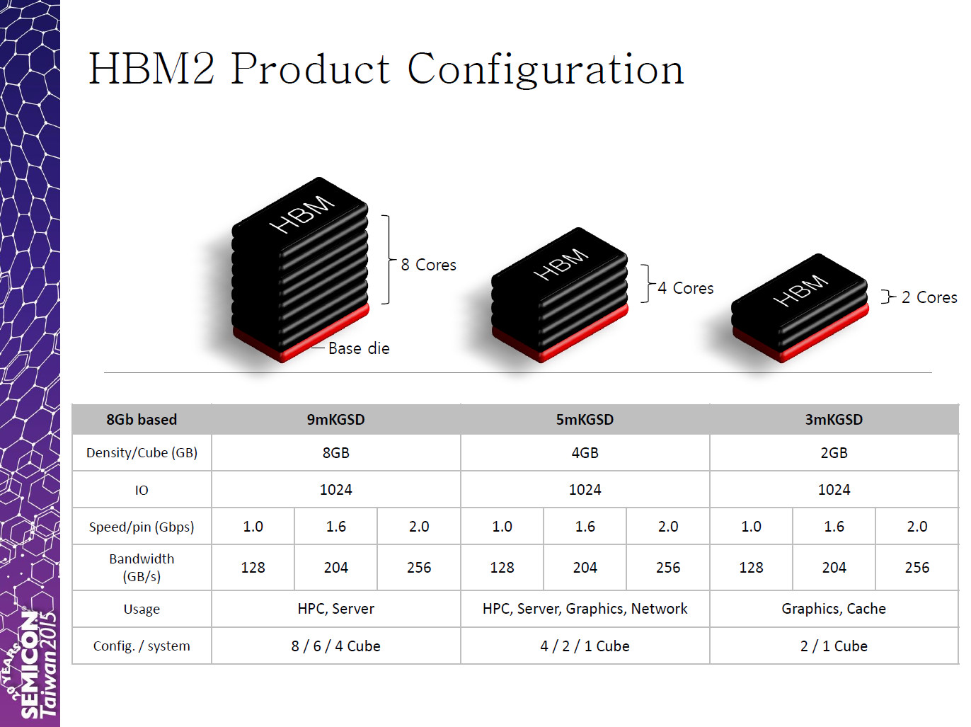
SK Hynix to Ship 4GB HBM2 Stacks by Q3-2016
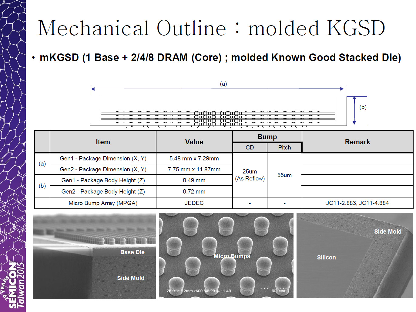
Korean DRAM and NAND flash giant SK Hynix will be ready to ship its 4 GB stacked second generation high-bandwidth memory (HBM2) chips from Q3, 2016. These packages will be made up of four 1 GB dies, with a bandwidth-per-pin of 1 Gbps, 1.6 Gbps, and 2 Gbps, working out to per-stack bandwidths of 128 GB/s, 204 GB/s, and 256 GB/s, respectively.
These chips will target applications such as graphics cards, network infrastructure, HPC, and servers. The company is also designing 8 GB stacks, made up of eight 1 GB dies. These stacks will be targeted at HPC and server applications. The company is also offering cost-effective 2 GB, 2-die stacks, for graphics cards. The cost-effective 2 GB, 2-die stacks could prove particularly important for the standard's competition against GDDR5X, particularly in mid-range and performance-segment graphics cards.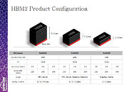
These chips will target applications such as graphics cards, network infrastructure, HPC, and servers. The company is also designing 8 GB stacks, made up of eight 1 GB dies. These stacks will be targeted at HPC and server applications. The company is also offering cost-effective 2 GB, 2-die stacks, for graphics cards. The cost-effective 2 GB, 2-die stacks could prove particularly important for the standard's competition against GDDR5X, particularly in mid-range and performance-segment graphics cards.