News Posts matching #HBM2

Return to Keyword Browsing

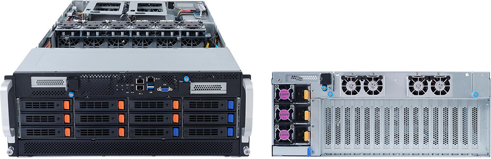
NVIDIA Launches A100 PCIe-Based Accelerator with 80 GB HBM2E Memory

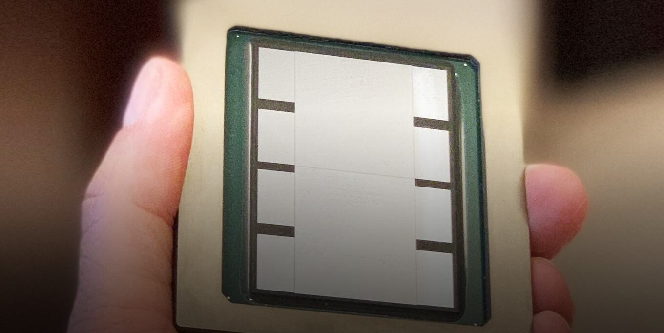
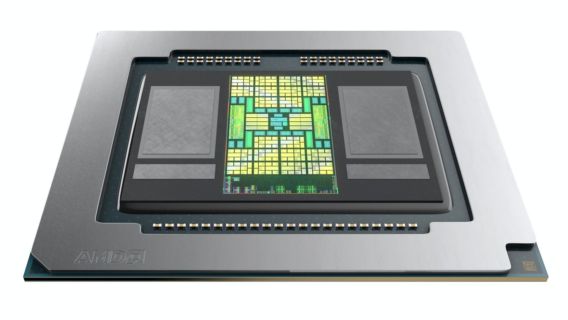
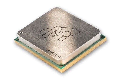
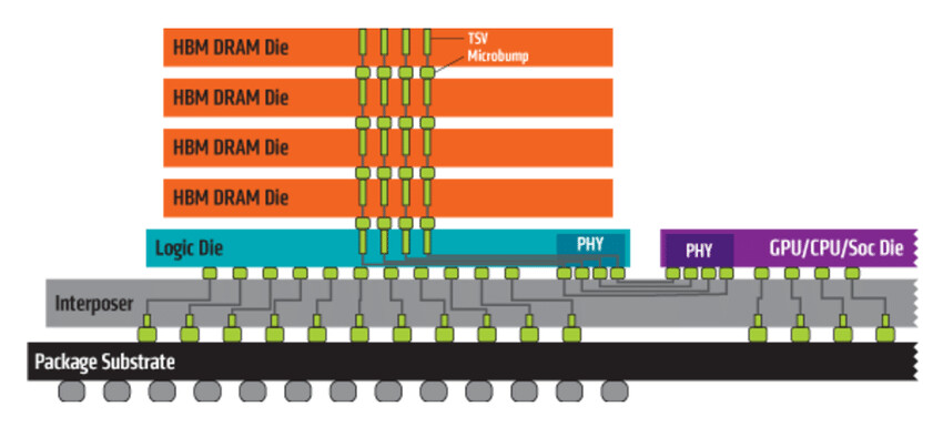
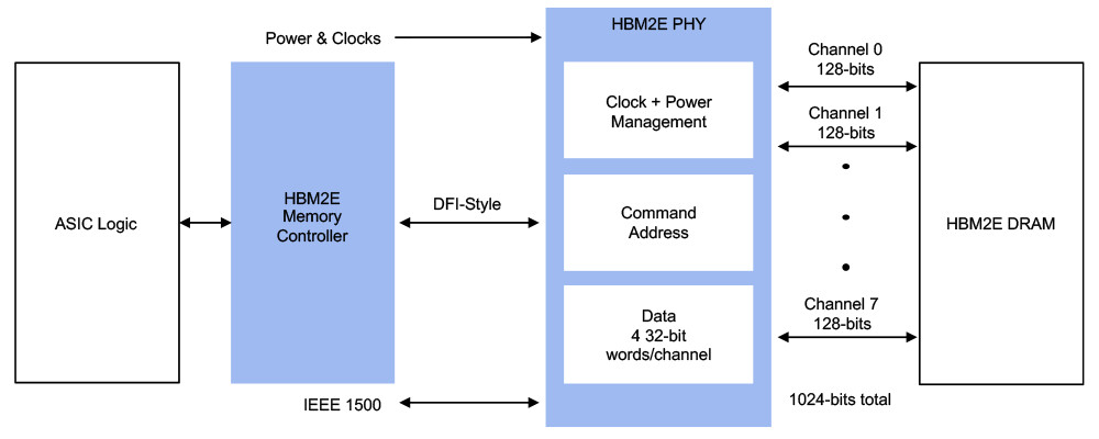
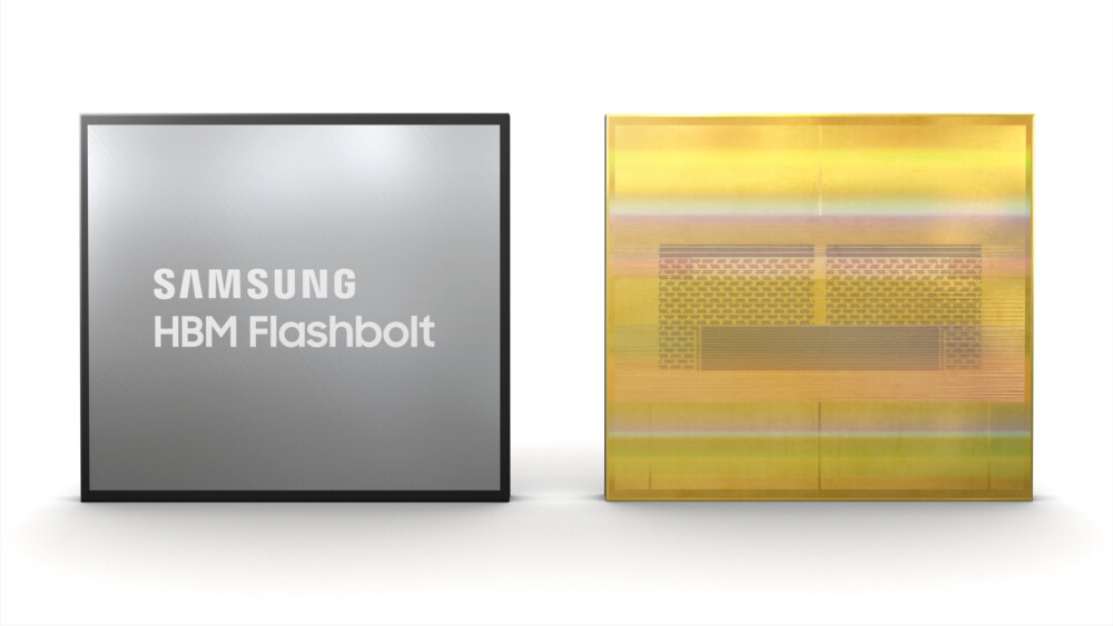
During this year's ISC 2021 event, as a part of the company's exhibition portfolio, NVIDIA has decided to launch an updated version of the A100 accelerator. A couple of months ago, in November, NVIDIA launched an 80 GB HBM2E version of the A100 accelerator, on the SXM2 proprietary form-factor. Today, we are getting the same upgraded GPU in the more standard dual-slot PCIe type of card. Featuring a GA100 GPU built on TSMC's 7 nm process, this SKU has 6192 CUDA cores present. To pair with the beefy amount of computing, the GPU needs appropriate memory. This time, there is as much as 80 GB of HBM2E memory. The memory achieves a bandwidth of 2039 GB/s, with memory dies running at an effective speed of 3186 Gbps. An important note is that the TDP of the GPU has been lowered to 250 Watts, compared to the 400 Watt SXM2 solution.

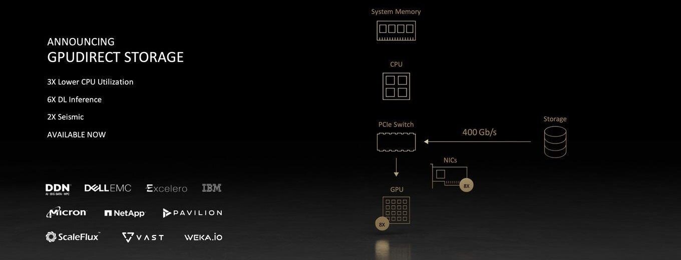
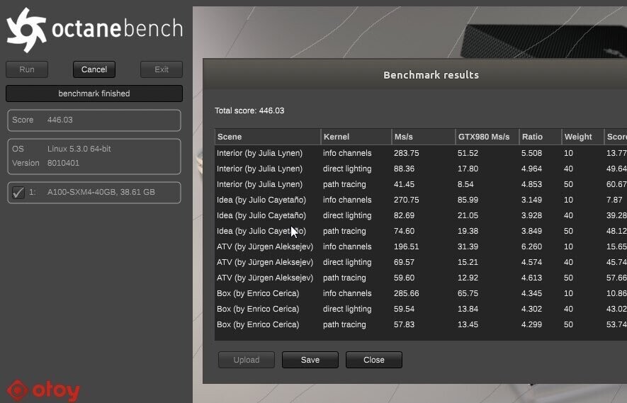
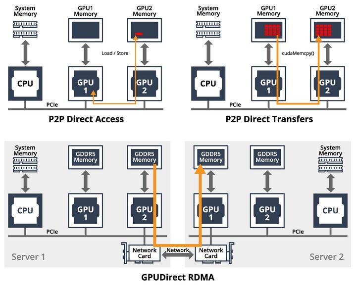
To pair with the new upgrade, NVIDIA made another announcement today and that is an enterprise version of Microsoft's DirectStorage, called NVIDIA GPUDirect Storage. It represents a way of allowing applications to access the massive memory pool built on the GPU, with 80 GB of super-fast HBM2E memory.

NVIDIA and Global Partners Launch New HGX A100 Systems to Accelerate Industrial AI and HPC

NVIDIA today announced it is turbocharging the NVIDIA HGX AI supercomputing platform with new technologies that fuse AI with high performance computing, making supercomputing more useful to a growing number of industries.

To accelerate the new era of industrial AI and HPC, NVIDIA has added three key technologies to its HGX platform: the NVIDIA A100 80 GB PCIe GPU, NVIDIA NDR 400G InfiniBand networking, and NVIDIA Magnum IO GPUDirect Storage software. Together, they provide the extreme performance to enable industrial HPC innovation.

Intel Xeon "Sapphire Rapids" Processor Die Shot Leaks

Thanks to the information coming from Yuuki_Ans, a person which has been leaking information about Intel's upcoming 4th generation Xeon Scalable processors codenamed Sapphire Rapids, we have the first die shots of the Sapphire Rapids processor and its delidded internals to look at. After performing the delidding process and sanding down the metal layers of the dies, the leaker has been able to take a few pictures of the dies present on the processor. As the Sapphire Rapids processor uses multi-chip modules (MCM) approach to building CPUs, the design is supposed to provide better yields for Intel and give the 10 nm dies better usability if defects happen.

In the die shots, we see that there are four dies side by side, with each die featuring 15 cores. That would amount to 60 cores present in the system, however, not all of the 60 cores are enabled. The top SKU is supposed to feature 56 cores, meaning that there would be at least four cores disabled across the configuration. This gives Intel flexibility to deliver plenty of processors, whatever the yields look like. The leaked CPU is an early engineering sample design with a low frequency of 1.3 GHz, which should improve in the final design. Notably, as Sapphire Rapids has SKUs that use in-package HBM2E memory, we don't know if the die configuration will look different from the one pictured down below.

AMD Confirms CDNA2 Instinct MI200 GPU Will Feature at Least Two Dies in MCM Design

Today we've got the first genuine piece of information that confirms AMD's MCM approach to CDNA2, the next-gen compute architecture meant for ML/HPC/Exascale computing. This comes courtesy of a Linux kernel update, where AMD engineers annotated the latest Linux kernel patch with some considerations specific for their upcoming Aldebaran, CDNA2-based compute cards. Namely, the engineers clarify the existence of a "Die0" and a "Die1", where power data fetching should be allocated to Die0 of the accelerator card - and that the power limit shouldn't be set on the secondary die.

This confirms that Aldebaran will be made of at least two CDNA2 compute dies, and as (almost) always in computing, one seems to be tasked with general administration of both compute dies. It is unclear as of yet whether the HBM2 memory controller will be allocated to the primary die, or if there will be an external I/O die (much like in Zen) that AMD can leverage for off-chip communication. AMD's approach to CDNA2 will eventually find its way (in an updated form) for AMD's consumer-geared next-generation graphics architecture with RDNA3.

NVIDIA and Global Computer Makers Launch Industry-Standard Enterprise Server Platforms for AI

NVIDIA today introduced a new class of NVIDIA-Certified Systems, bringing AI within reach for organizations that run their applications on industry-standard enterprise data center infrastructure. These include high-volume enterprise servers from top manufacturers, which were announced in January and are now certified to run the NVIDIA AI Enterprise software suite—which is exclusively certified for VMware vSphere 7, the world's most widely used compute virtualization platform.

Further expanding the NVIDIA-Certified servers ecosystem is a new wave of systems featuring the NVIDIA A30 GPU for mainstream AI and data analytics and the NVIDIA A10 GPU for AI-enabled graphics, virtual workstations and mixed compute and graphics workloads, also announced today.

Intel's Upcoming Sapphire Rapids Server Processors to Feature up to 56 Cores with HBM Memory

Intel has just launched its Ice Lake-SP lineup of Xeon Scalable processors, featuring the new Sunny Cove CPU core design. Built on the 10 nm node, these processors represent Intel's first 10 nm shipping product designed for enterprise. However, there is another 10 nm product going to be released for enterprise users. Intel is already preparing the Sapphire Rapids generation of Xeon processors and today we get to see more details about it. Thanks to the anonymous tip that VideoCardz received, we have a bit more details like core count, memory configurations, and connectivity options. And Sapphire Rapids is shaping up to be a very competitive platform. Do note that the slide is a bit older, however, it contains useful information.

The lineup will top at 56 cores with 112 threads, where this processor will carry a TDP of 350 Watts, notably higher than its predecessors. Perhaps one of the most interesting notes from the slide is the department of memory. The new platform will make a debut of DDR5 standard and bring higher capacities with higher speeds. Along with the new protocol, the chiplet design of Sapphire Rapids will bring HBM2E memory to CPUs, with up to 64 GBs of it per socket/processor. The PCIe 5.0 standard will also be present with 80 lanes, accompanying four Intel UPI 2.0 links. Intel is also supposed to extend the x86_64 configuration here with AMX/TMUL extensions for better INT8 and BFloat16 processing.

AMD is Preparing RDNA-Based Cryptomining GPU SKUs

Back in February, NVIDIA has announced its GPU SKUs dedicated to the cryptocurrency mining task, without any graphics outputs present on the chips. Today, we are getting information that AMD is rumored to introduce its own lineup of graphics cards dedicated to cryptocurrency mining. In the latest patch for AMD Direct Rendering Manager (DRM), a subsystem of the Linux kernel responsible for interfacing with GPUs, we see the appearance of the Navi 12. This GPU SKU was not used for anything except Apple's Mac devices in a form of Radeon Pro 5600M GPU. However, it seems like the Navi 12 could join forces with Navi 10 GPU SKU and become a part of special "blockchain" GPUs.

Way back in November, popular hardware leaker, KOMACHI, has noted that AMD is preparing three additional Radeon SKUs called Radeon RX 5700XTB, RX 5700B, and RX 5500XTB. The "B" added to the end of each name is denoting the blockchain revision, made specifically for crypto-mining. When it comes to specifications of the upcoming mining-specific AMD GPUs, we know that both use first-generation RDNA architecture and have 2560 Stream Processors (40 Compute Units). Memory configuration for these cards remains unknown, as AMD surely won't be putting HBM2 stacks for mining like it did with Navi 12 GPU. All that remains is to wait and see what AMD announces in the coming months.

SiPearl to Manufacture its 72-Core Rhea HPC SoC at TSMC Facilities

SiPearl has this week announced their collaboration with Open-Silicon Research, the India-based entity of OpenFive, to produce the next-generation SoC designed for HPC purposes. SiPearl is a part of the European Processor Initiative (EPI) team and is responsible for designing the SoC itself that is supposed to be a base for the European exascale supercomputer. In the partnership with Open-Silicon Research, SiPearl expects to get a service that will integrate all the IP blocks and help with the tape out of the chip once it is done. There is a deadline set for the year 2023, however, both companies expect the chip to get shipped by Q4 of 2022.

When it comes to details of the SoC, it is called Rhea and it will be a 72-core Arm ISA based processor with Neoverse Zeus cores interconnected by a mesh. There are going to be 68 mesh network L3 cache slices in between all of the cores. All of that will be manufactured using TSMC's 6 nm extreme ultraviolet lithography (EUV) technology for silicon manufacturing. The Rhea SoC design will utilize 2.5D packaging with many IP blocks stitched together and HBM2E memory present on the die. It is unknown exactly what configuration of HBM2E is going to be present. The system will also see support for DDR5 memory and thus enable two-level system memory by combining HBM and DDR. We are excited to see how the final product looks like and now we wait for more updates on the project.

TSMC to Enter Mass Production of 6th Generation CoWoS Packaging in 2023, up to 12 HBM Stacks

TSMC, the world's leading semiconductor manufacturing company, is rumored to start production of its 6th generation Chip-on-Wafer-on-Substrate (CoWoS) packaging technology. As the silicon scaling is getting ever so challenging, the manufacturers have to come up with a way to get as much performance as possible. That is where TSMC's CoWoS and other chiplet technologies come. They allow designers to integrate many integrated circuits on a single package, making for a cheaper overall product compared to if the product used one big die. So what is so special about 6th generation CoWoS technology from TSMC, you might wonder. The new generation is said to enable a massive 12 stacks of HBM memory on a package. You are reading that right. Imagine if each stack would be an HBM2E variant with 16 GB capacity that would be 192 GB of memory on the package present. Of course, that would be a very expensive chip to manufacture, however, it is just a showcase of what the technology could achieve.

Update 16:44 UTC—TheEnglish DigiTimes report indicates that this technology is expected to see mass production in 2023.

Rambus Advances HBM2E Performance to 4.0 Gbps for AI/ML Training Applications

Rambus Inc. (NASDAQ: RMBS), a premier silicon IP and chip provider making data faster and safer, today announced it has achieved a record 4 Gbps performance with the Rambus HBM2E memory interface solution consisting of a fully-integrated PHY and controller. Paired with the industry's fastest HBM2E DRAM from SK hynix operating at 3.6 Gbps, the solution can deliver 460 GB/s of bandwidth from a single HBM2E device. This performance meets the terabyte-scale bandwidth needs of accelerators targeting the most demanding AI/ML training and high-performance computing (HPC) applications.

"With this achievement by Rambus, designers of AI and HPC systems can now implement systems using the world's fastest HBM2E DRAM running at 3.6 Gbps from SK hynix," said Uksong Kang, vice president of product planning at SK hynix. "In July, we announced full-scale mass-production of HBM2E for state-of-the-art computing applications demanding the highest bandwidth available."

NVIDIA Ampere A100 GPU Gets Benchmark and Takes the Crown of the Fastest GPU in the World

When NVIDIA introduced its Ampere A100 GPU, it was said to be the company's fastest creation yet. However, we didn't know how fast the GPU exactly is. With the whopping 6912 CUDA cores, the GPU can pack all that on a 7 nm die with 54 billion transistors. Paired with 40 GB of super-fast HBM2E memory with a bandwidth of 1555 GB/s, the GPU is set to be a good performer. And how fast it exactly is you might wonder? Well, thanks to the Jules Urbach, the CEO of OTOY, a software developer and maker of OctaneRender software, we have the first benchmark of the Ampere A100 GPU.

Scoring 446 points in OctaneBench, a benchmark for OctaneRender, the Ampere GPU takes the crown of the world's fastest GPU. The GeForce RTX 2080 Ti GPU scores 302 points, which makes the A100 GPU up to 47.7% faster than Turing. However, the fastest Turing card found in the benchmark database is the Quadro RTX 8000, which scored 328 points, showing that Turing is still holding well. The result of Ampere A100 was running with RTX turned off, which could yield additional performance if RTX was turned on and that part of the silicon started working.

GIGABYTE Introduces a Broad Portfolio of G-series Servers Powered by NVIDIA A100 PCIe

GIGABYTE, an industry leader in high-performance servers and workstations, announced its G-series servers' validation plan. Following the NVIDIA A100 PCIe GPU announcement today, GIGABYTE has completed the compatibility validation of the G481-HA0 / G292-Z40 and added the NVIDIA A100 to the support list for these two servers. The remaining G-series servers will be divided into two waves to complete their respective compatibility tests soon. At the same time, GIGABYTE also launched a new G492 series server based on the AMD EPYC 7002 processor family, which provides PCIe Gen4 support for up to 10 NVIDIA A100 PCIe GPUs. The G492 is a server with the highest computing power for AI models training on the market today. GIGABYTE will offer two SKUs for the G492. The G492-Z50 will be at a more approachable price point, whereas the G492-Z51 will be geared towards higher performance.

The G492 is GIGABYTE's second-generation 4U G-series server. Based on the first generation G481 (Intel architecture) / G482 (AMD architecture) servers, the user-friendly design and scalability have been further optimized. In addition to supporting two 280 W 2nd Gen AMD EPYC 7002 processors, the 32 DDR4 memory slots support up to 8 TB of memory and maintain data transmission at 3200 MHz. The G492 has built-in PCIe Gen4 switches, which can provide more PCIe Gen4 lanes. PCIe Gen4 has twice the I/O performance of PCIe Gen3 and fully enables the computing power of the NVIDIA A100 Tensor Core GPU, or it can be applied to PCIe storage to help provide a storage upgrade path that is native to the G492.

NVIDIA Announces A100 PCIe Tensor Core Accelerator Based on Ampere Architecture

NVIDIA and partners today announced a new way for interested users to partake in the AI-training capabilities of their Ampere graphics architecture in the form of the A100 PCIe. Diving a little deeper, and as the name implies, this solution differs from the SXM form-factor in that it can be deployed through systems' existing PCIe slots. The change in interface comes with a reduction in TDP from 400 W down to 250 W in the PCIe version - and equivalent reduced performance.

NVIDIA says peak throughput is the same across the SXM and PCIe version of their A100 accelerator. The difference comes in sustained workloads, where NVIDIA quotes the A100 as delivering 10% less performance compared to its SXM brethren. The A100 PCIe comes with the same 2.4 Gbps, 40 GB HBM2 memory footprint as the SXM version, and all other chip resources are the same. We're thus looking at the same 862 mm² silicon chip and 6,192 CUDA cores across both models. The difference is that the PCIe accelerator can more easily be integrated in existing server infrastructure.

AMD Radeon Pro 5600M with HBM2 Benchmarked

Benchmarks of the new Apple-exclusive AMD Radeon Pro 5600M graphics solution by Max Tech reveals that the new GPU is about 50% faster than the Radeon Pro 5500M, and within striking distance of the Radeon Pro Vega 48 found in Apple's 5K iMacs. The Pro 5600M is an Apple-exclusive solution by AMD, based on the "Navi 12" silicon that features a 7 nm GPU die based on the RDNA graphics architecture, flanked by two 4 GB HBM2 memory stacks over a 2048-bit interface. The GPU die features 2,560 stream processors, but clocked differently from Radeon Pro discrete graphics cards based on the "Navi 10" ASIC that uses conventional GDDR6.

The Radeon Pro 5600M solution was found to be 50.1 percent faster than the Radeon Pro 5500M in Geekbench 5 Metal (another Apple-exclusive SKU found in 16-inch MacBook Pros), and just 12.9 percent behind the Radeon Vega 48. The Vega 56 found in iMac Pro is still ahead. Unigine Heaven sees the Pro 5600M being 48.1% faster than the Pro 5500M, and interestingly, faster than Vega 48 by 11.3%. With 2,560 RDNA stream processors, you'd expect more performance, but this card was designed to meet stringent power limits of 50 W, and has significantly lower clock-speeds than "Navi 10" based Radeon Pro graphics cards (1035 MHz max boost engine clock vs. 1930 MHz and 205 W TDP of the Pro W5700). Find more interesting commentary in the Max Tech video presentation.

AMD "Navi 12" Silicon Powering the Radeon Pro 5600M Rendered

Out of the blue, AMD announced its Radeon Pro 5600M mobile discrete graphics solution exclusive for Apple's 16-inch MacBook Pro. It turns out that the Pro 5600M is based on an all new ASIC by AMD, codenamed "Navi 12." This is a multi-chip module, much like "Vega 20," featuring a 7 nm GPU die and two 16 Gbit (4 GB) HBM2 memory stacks sitting on an interposer. While the actual specs of the GPU die on the "Navi 14" aren't known, on the Pro 5600M, it is configured with 40 RDNA compute units amounting to 2,560 stream processors, 160 TMUs, and possibly 64 ROPs.

The engine clock of the Pro 5600M is set at up to 1035 MHz. The HBM2 memory is clocked at 1.54 Gbps, which at the 2048-bit bus width, translates to 394 GB/s of memory bandwidth. There are two big takeaways from this expensive-looking ASIC design: a significantly smaller PCB footprint compared to a "Navi 10" ASIC with its eight GDDR6 memory chips; and a significantly lower power envelope. AMD rates the typical power at just 50 W. In the render below, the new ASIC is shown next to a "Navi 14" ASIC that power RX/Pro 5500-series SKUs.

New AMD Radeon Pro 5600M Mobile GPU Brings Desktop-Class Graphics Performance and Enhanced Power Efficiency to 16-inch MacBook Pro

AMD today announced availability of the new AMD Radeon Pro 5600M mobile GPU for the 16-inch MacBook Pro. Designed to deliver desktop-class graphics performance in an efficient mobile form factor, this new GPU powers computationally heavy workloads, enabling pro users to maximize productivity while on-the-go.

The AMD Radeon Pro 5600M GPU is built upon industry-leading 7 nm process technology and advanced AMD RDNA architecture to power a diverse range of pro applications, including video editing, color grading, application development, game creation and more. With 40 compute units and 8 GB of ultra-fast, low-power High Bandwidth Memory (HBM2), the AMD Radeon Pro 5600M GPU delivers superfast performance and excellent power efficiency in a single GPU package.

NVIDIA Tesla A100 "Ampere" AIC (add-in card) Form-Factor Board Pictured

Here's the first picture of a Tesla A100 "Ampere" AIC (add-in card) form-factor board, hot on the heals of the morning big A100 reveal. The AIC card is a bare PCB, which workstation builders will add compatible cooling solutions on. The PCB features the gigantic GA100 processor with its six HBM2E stacks, in the center, surrounded by VRM components, and I/O on three sides. On the bottom side, you will find a conventional PCI-Express 4.0 x16 host interface. Above it, are NVLink fingers. The rear I/O has high-bandwidth network interfaces (likely 200 Gbps InfiniBand), by Mellanox. The tail end has hard points for 12 V power input. Find juicy details of the GA100 in our older article.

NVIDIA Tesla A100 GPU Pictured

Thanks to the sources of VideoCardz, we now have the first picture of the next-generation NVIDIA Tesla A100 graphics card. Designed for computing oriented applications, the Tesla A100 is a socketed GPU designed for NVIDIA's proprietary SXM socket. In a post few days ago, we were suspecting that you might be able to fit the Tesla A100 GPU in the socket of the previous Volta V100 GPUs as it is a similar SXM socket. However, the mounting holes have been re-arranged and this one requires a new socket/motherboard. The Tesla A100 GPU is based on GA100 GPU die, which we don't know specifications of. From the picture, we can only see that there is one very big die attached to six HBM modules, most likely HBM2E. Besides that everything else is unknown. More details are expected to be announced today at the GTC 2020 digital keynote.
NVIDIA Tesla A100

AMD Announces Radeon Pro VII Graphics Card, Brings Back Multi-GPU Bridge

AMD today announced its Radeon Pro VII professional graphics card targeting 3D artists, engineering professionals, broadcast media professionals, and HPC researchers. The card is based on AMD's "Vega 20" multi-chip module that incorporates a 7 nm (TSMC N7) GPU die, along with a 4096-bit wide HBM2 memory interface, and four memory stacks adding up to 16 GB of video memory. The GPU die is configured with 3,840 stream processors across 60 compute units, 240 TMUs, and 64 ROPs. The card is built in a workstation-optimized add-on card form-factor (rear-facing power connectors and lateral-blower cooling solution).

What separates the Radeon Pro VII from last year's Radeon VII is full double precision floating point support, which is 1:2 FP32 throughput compared to the Radeon VII, which is locked to 1:4 FP32. Specifically, the Radeon Pro VII offers 6.55 TFLOPs double-precision floating point performance (vs. 3.36 TFLOPs on the Radeon VII). Another major difference is the physical Infinity Fabric bridge interface, which lets you pair up to two of these cards in a multi-GPU setup to double the memory capacity, to 32 GB. Each GPU has two Infinity Fabric links, running at 1333 MHz, with a per-direction bandwidth of 42 GB/s. This brings the total bidirectional bandwidth to a whopping 168 GB/s—more than twice the PCIe 4.0 x16 limit of 64 GB/s.

Fujitsu Completes Delivery of Fugaku Supercomputer

Fujitsu has today officially completed the delivery of the Fugaku supercomputer to the Riken scientific research institute of Japan. This is a big accomplishment as the current COVID-19 pandemic has delayed many happenings in the industry. However, Fujitsu managed to play around that and deliver the supercomputer on time. The last of 400 racks needed for the Fugaku supercomputer was delivered today, on May 13th, as it was originally planned. The supercomputer is supposed to be fully operational starting on the physical year of 2021, where the installation and setup will be done before.

As a reminder, the Fugaku is an Arm-based supercomputer consisting out of 150 thousand A64FX CPUs. These CPUs are custom made processors by Fujitsu based on Arm v8.2 ISA, and they feature 48 cores built on TSMC 7 nm node and running above 2 GHz. Packing 8.786 billion transistors, this monster chips use HBM2 memory instead of a regular DDR memory interface. Recently, a prototype of the Fugaku supercomputer was submitted to the Top500 supercomputer list and it came on top for being the most energy-efficient of all, meaning that it will be as energy efficient as it will be fast. Speculations are that it will have around 400 PetaFlops of general compute power for Dual-Precision workloads, however, for the specific artificial intelligence applications, it should achieve ExaFLOP performance target.
K SuperComputer

Micron to Launch HBM2 Memory This Year

Micron Technologies, in the latest earnings report, announced that they will start shipping High-Bandwidth Memory 2 (HBM2) DRAM. Used for high-performance graphics cards, server processors and all kinds of processors, HBM2 memory is wanted and relatively expensive solution, however, when Micron enters the market of its manufacturing, prices, and the market should adjust for the new player. Previously, only SK-Hynix and Samsung were manufacturing the HBM2 DRAM, however, Micron will join them and they will again form a "big-three" pact that dominates the memory market.

Up until now, Micron used to lay all hopes on its proprietary Hybrid Memory Cube (HMC) DRAM type, which didn't gain much traction from customers and it never really took off. Only a few rare products used it, as Fujitsu SPARC64 XIfx CPU used in Fujitsu PRIMEHPC FX100 supercomputer introduced in 2015. Micron announced to suspend works on HMC in 2018 and decided to devote their efforts to GDDR6 and HBM development. So, as a result, we are seeing that they will launch HBM2 DRAM products sometime this year.
Micron HMC High-Bandwidth Memory

Rambus Designs HBM2E Controller and PHY

Rambus, a maker of various Interface IP solutions, today announced the latest addition to its high-speed memory interface IP product portfolio in form of High Bandwidth Memory 2E (HBM2E) controller and physical layer (PHY) IP solution. The two IPs are enabling customers to completely integrate the HBM2E memory into their products, given that Rambus provides a complete solution for controlling and interfacing the memory. The design that Ramus offers can support for 12-high DRAM stacks of up to 24 Gb devices, making for up to 36 GB of memory per 3D stack. This single 3D stack is capable of delivering 3.2 Gbps over a 1024-bit wide interface, delivering 410 GB/s of bandwidth per stack.

The HBM2E controller core is DFI 3.1 compatible and has support for logic interfaces like AXI, OCP, or a custom one, so the customer can choose a way to integrate this core in their design. With a purchase of their HBM2E IP, Rambus will provide source code written in Hardware Description Language (HDL) and GDSII file containing the layout of the interface.

AMD Announces the CDNA and CDNA2 Compute GPU Architectures

AMD at its 2020 Financial Analyst Day event unveiled its upcoming CDNA GPU-based compute accelerator architecture. CDNA will complement the company's graphics-oriented RDNA architecture. While RDNA powers the company's Radeon Pro and Radeon RX client- and enterprise graphics products, CDNA will power compute accelerators such as Radeon Instinct, etc. AMD is having to fork its graphics IP to RDNA and CDNA due to what it described as market-based product differentiation.

Data centers and HPCs using Radeon Instinct accelerators have no use for the GPU's actual graphics rendering capabilities. And so, at a silicon level, AMD is removing the raster graphics hardware, the display and multimedia engines, and other associated components that otherwise take up significant amounts of die area. In their place, AMD is adding fixed-function tensor compute hardware, similar to the tensor cores on certain NVIDIA GPUs.
AMD Datacenter GPU Roadmap CDNA CDNA2 AMD CDNA Architecture AMD Exascale Supercomputer

AMD Radeon Instinct MI100 "Arcturus" Hits the Radar, We Have its BIOS

AMD's upcoming large post-Navi graphics chip, codenamed "Arcturus," will debut as "Radeon Instinct MI100", which is an AI-ML accelerator under the Radeon Instinct brand, which AMD calls "Server Accelerators." TechPowerUp accessed its BIOS, which is now up on our VGA BIOS database. The card goes with the device ID "0x1002 0x738C," which confirms "AMD" and "Arcturus,". The BIOS also confirms that memory size is at a massive 32 GB HBM2, clocked at 1000 MHz real (possibly 1 TB/s bandwidth, if memory bus width is 4096-bit).

Both Samsung (KHA884901X) and Hynix memory (H5VR64ESA8H) is supported, which is an important capability for AMD's supply chain. From the ID string "MI100 D34303 A1 XL 200W 32GB 1000m" we can derive that the TDP limit is set to a surprisingly low 200 W, especially considering this is a 128 CU / 8,192 shader count design. Vega 64 and Radeon Instinct MI60 for comparison have around 300 W power budget with 4,096 shaders, 5700 XT has 225 W with 2560 shaders, so either AMD achieved some monumental efficiency improvements with Arcturus or the whole design is intentionally running constrained, so that AMD doesn't reveal their hand to these partners, doing early testing of the card.

Samsung Launches 3rd-Generation "Flashbolt" HBM2E Memory

Samsung Electronics, the world leader in advanced memory technology, today announced the market launch of 'Flashbolt', its third-generation High Bandwidth Memory 2E (HBM2E). The new 16-gigabyte (GB) HBM2E is uniquely suited to maximize high performance computing (HPC) systems and help system manufacturers to advance their supercomputers, AI-driven data analytics and state-of-the-art graphics systems in a timely manner.

"With the introduction of the highest performing DRAM available today, we are taking a critical step to enhance our role as the leading innovator in the fast-growing premium memory market," said Cheol Choi, executive vice president of Memory Sales & Marketing at Samsung Electronics. "Samsung will continue to deliver on its commitment to bring truly differentiated solutions as we reinforce our edge in the global memory marketplace."
Return to Keyword Browsing
May 21st, 2024 07:00 EDT change timezone

New Forum Posts

Popular Reviews

Controversial News Posts