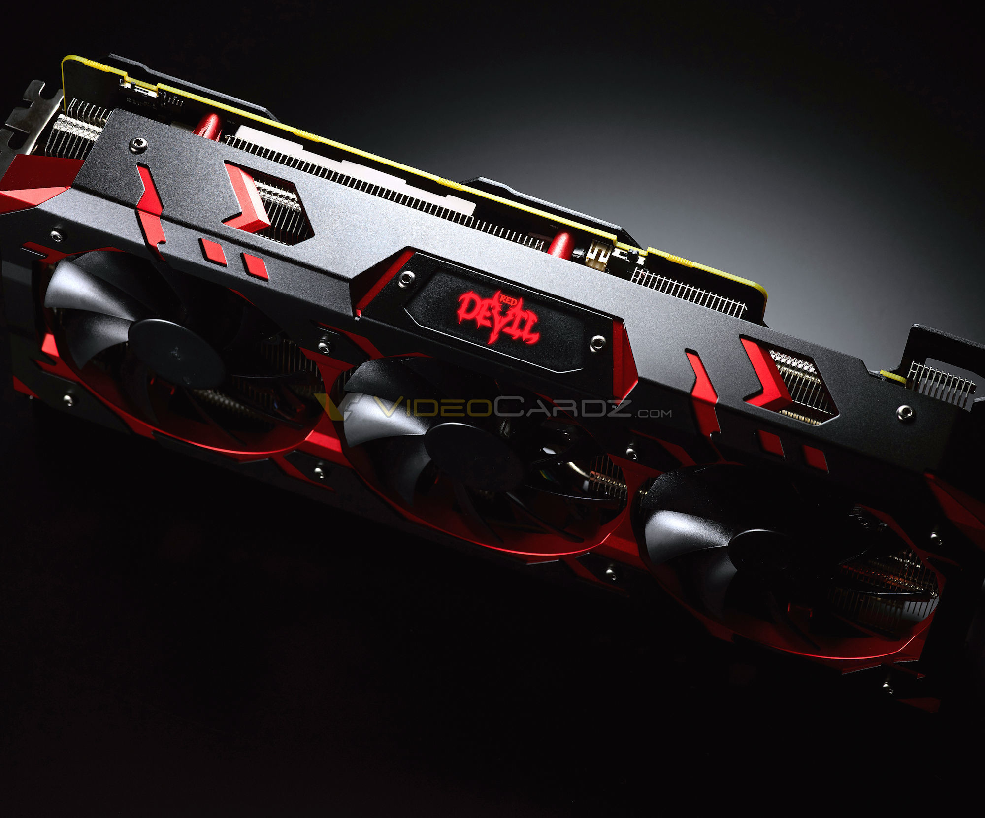
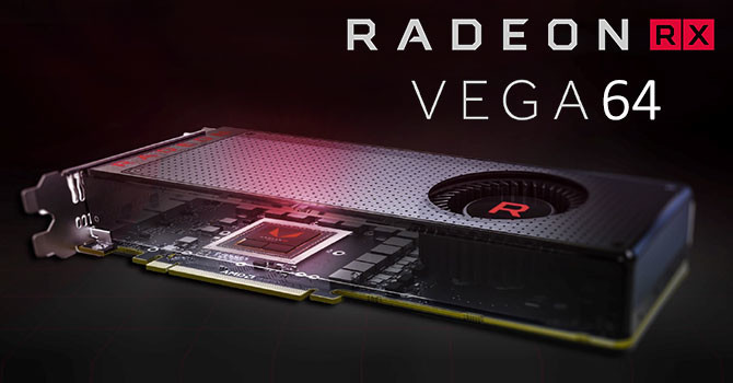
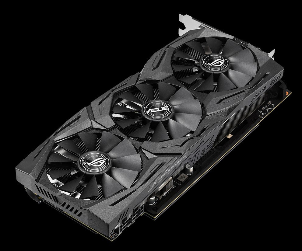
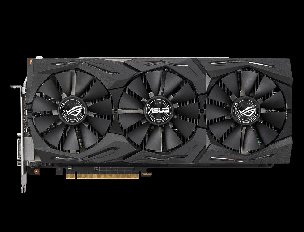
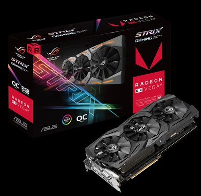
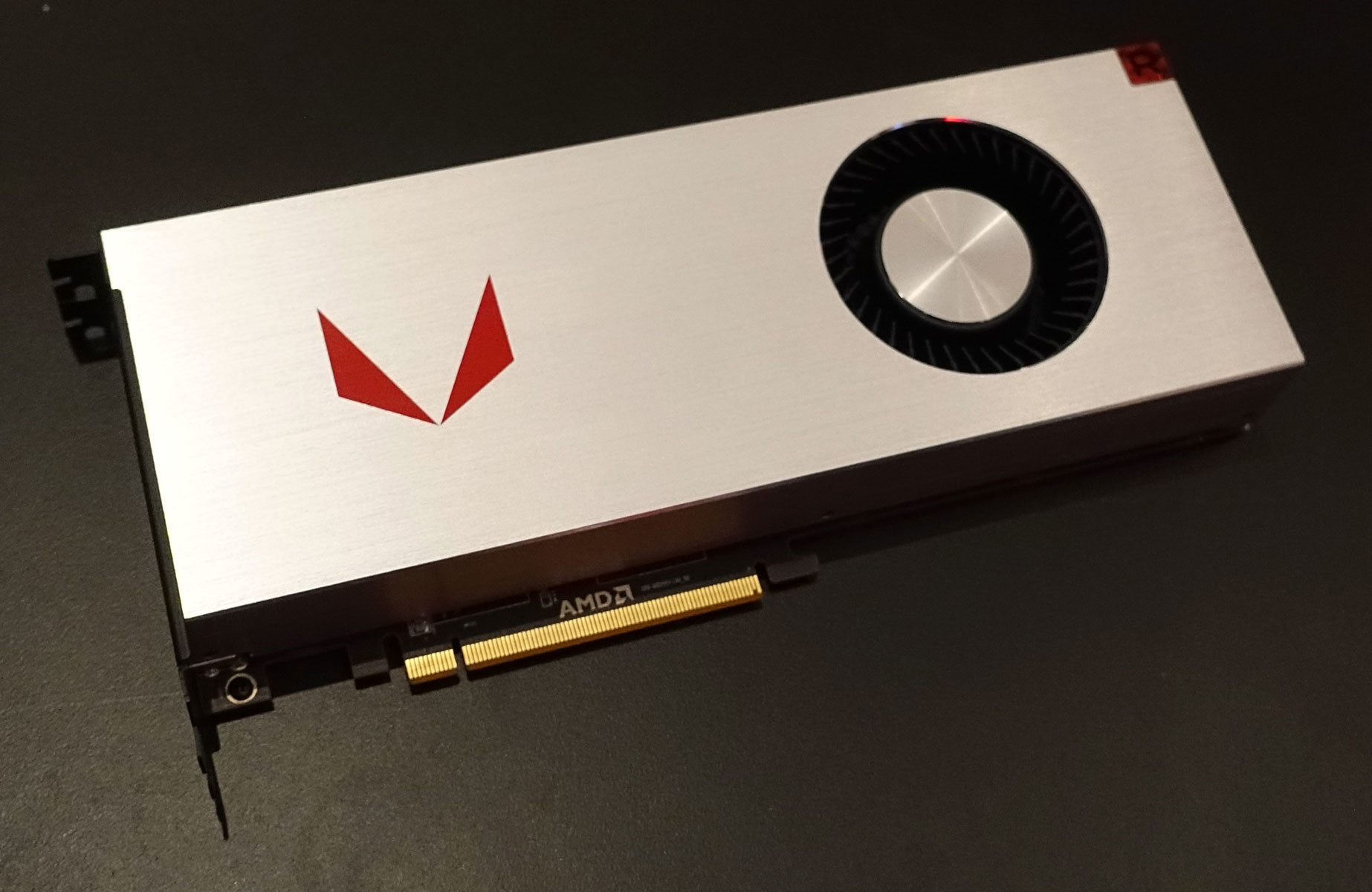
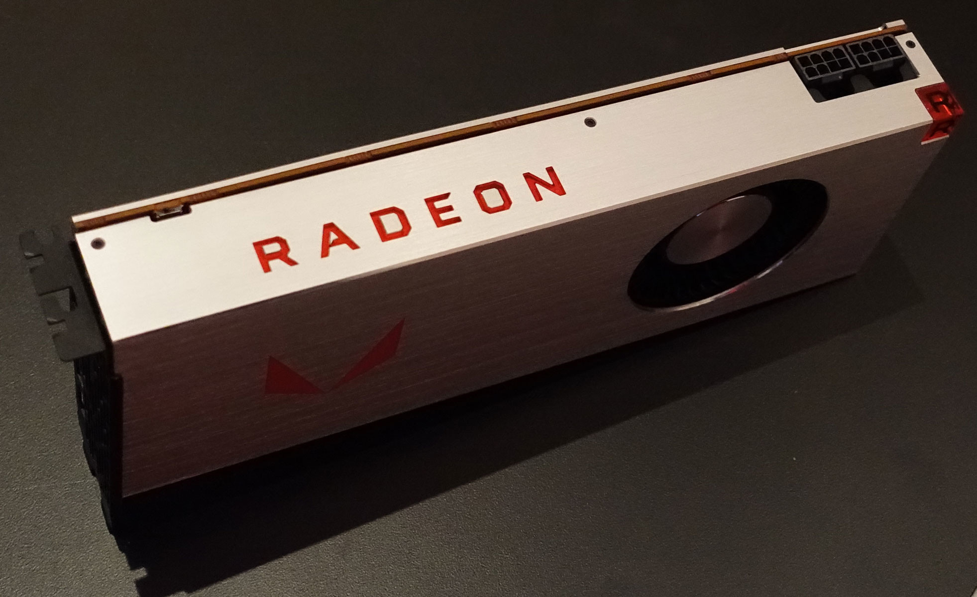
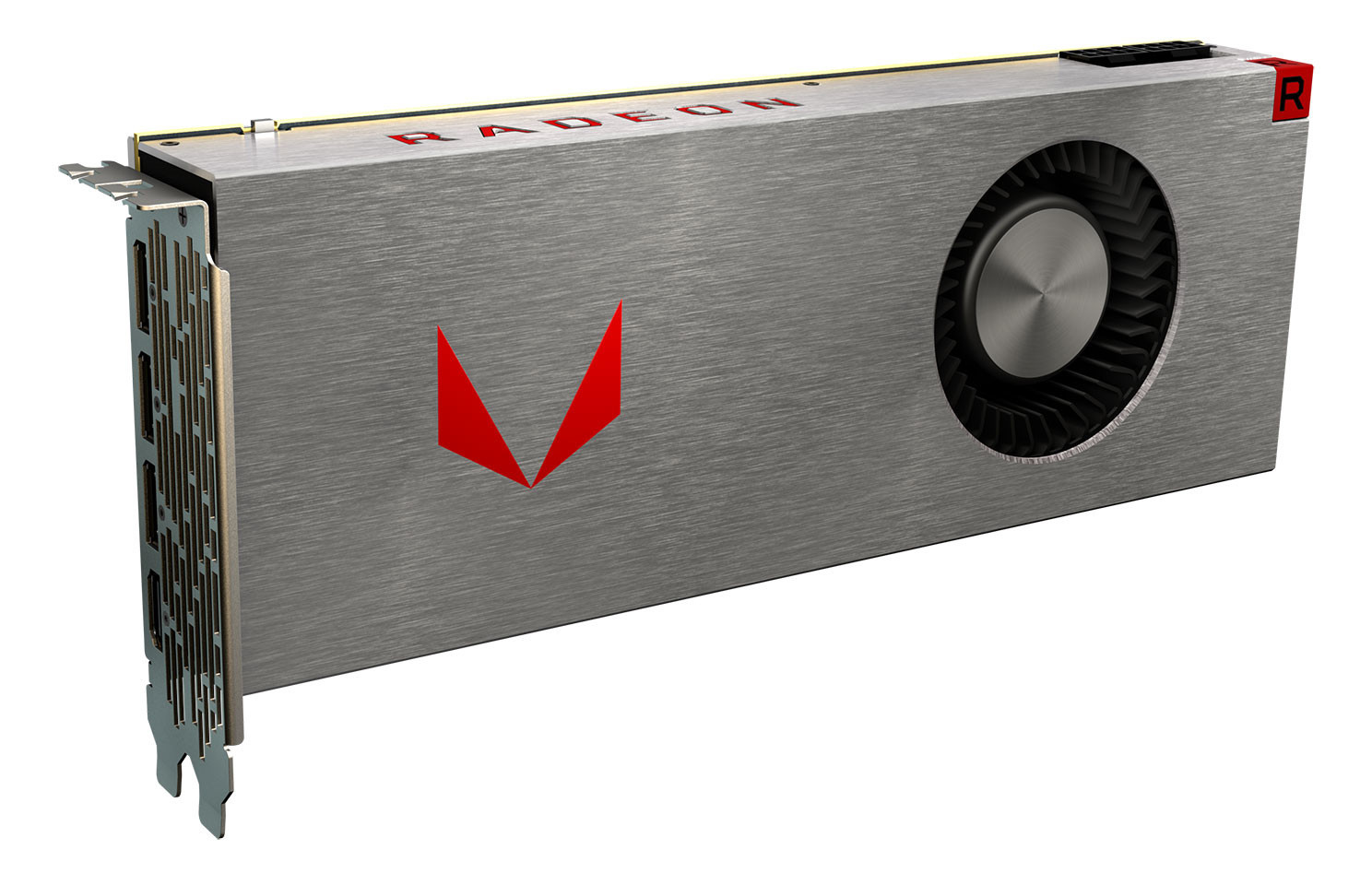
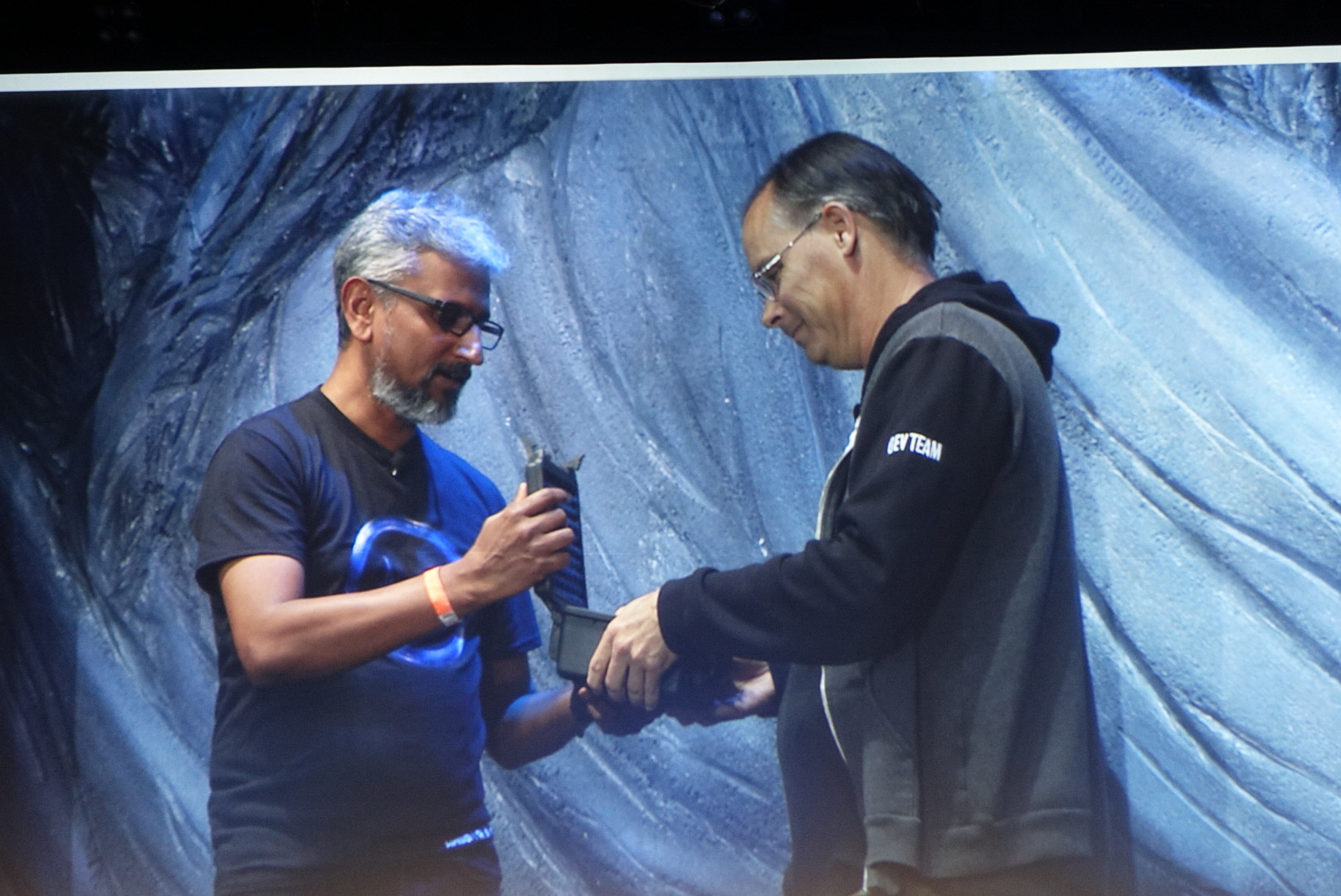
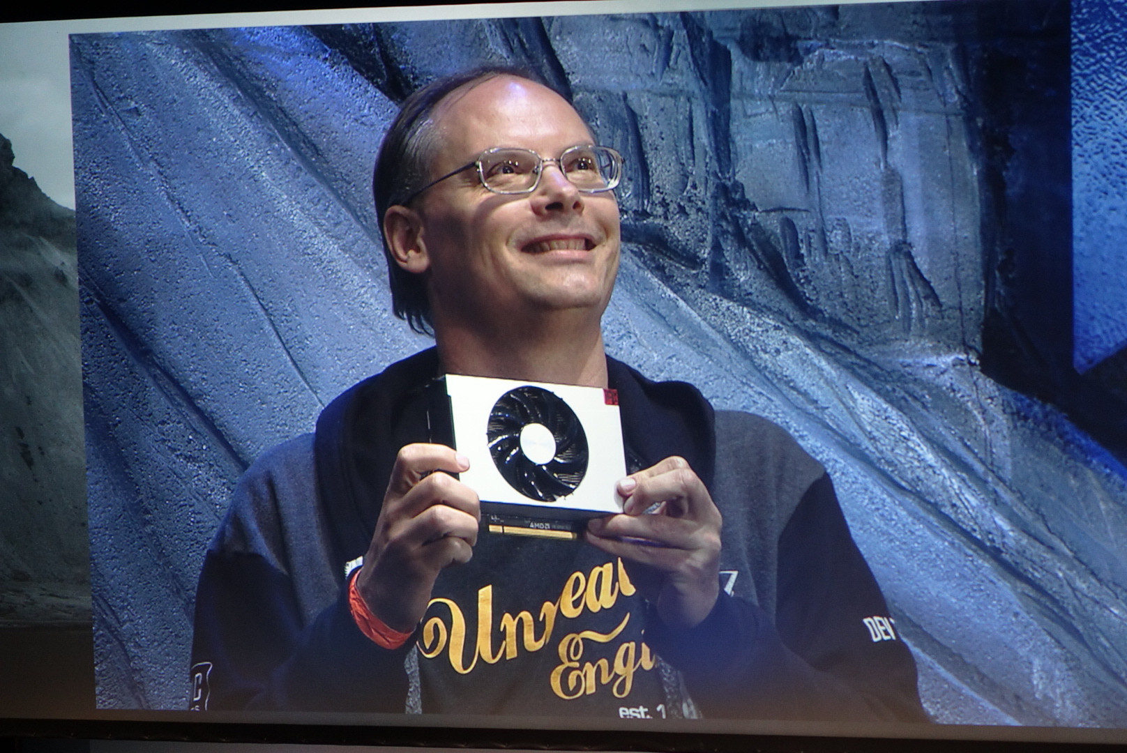
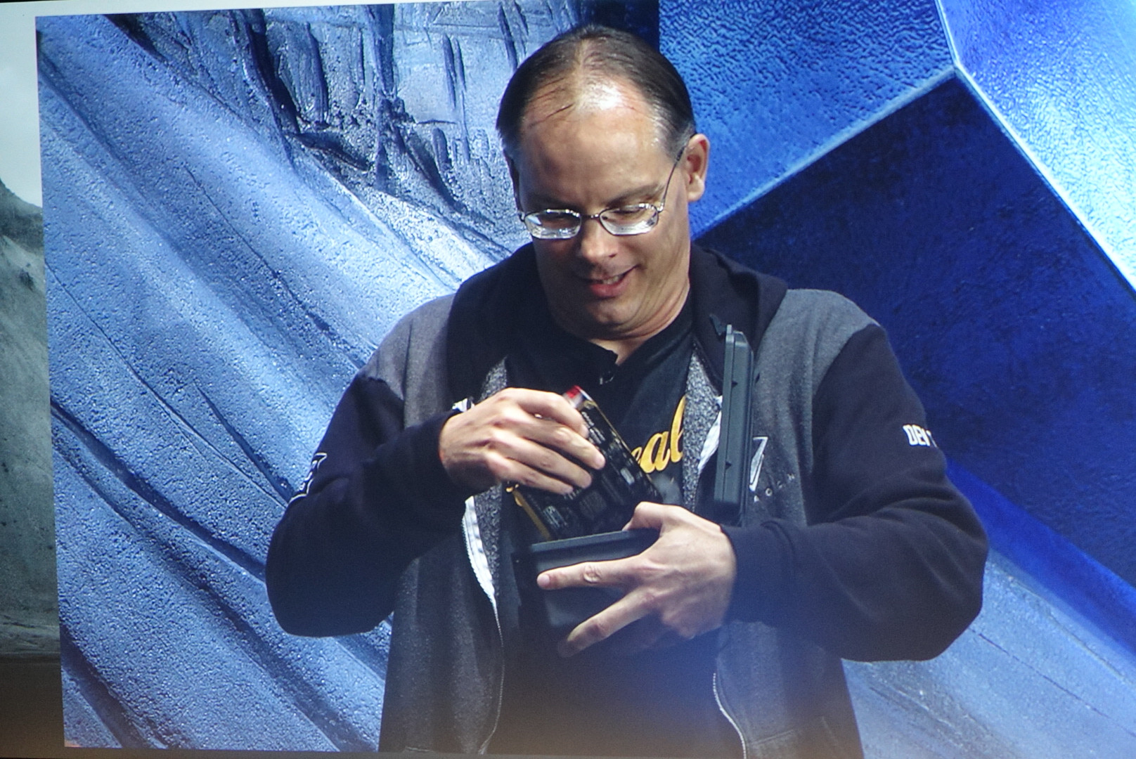
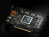
PowerColor Radeon RX Vega 64 Red Devil Available Soon, Overclocked, £590
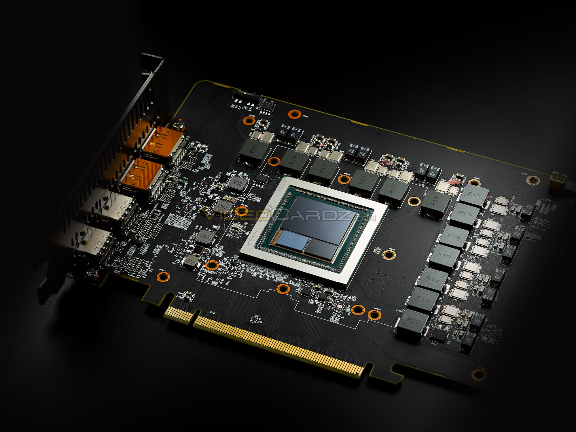
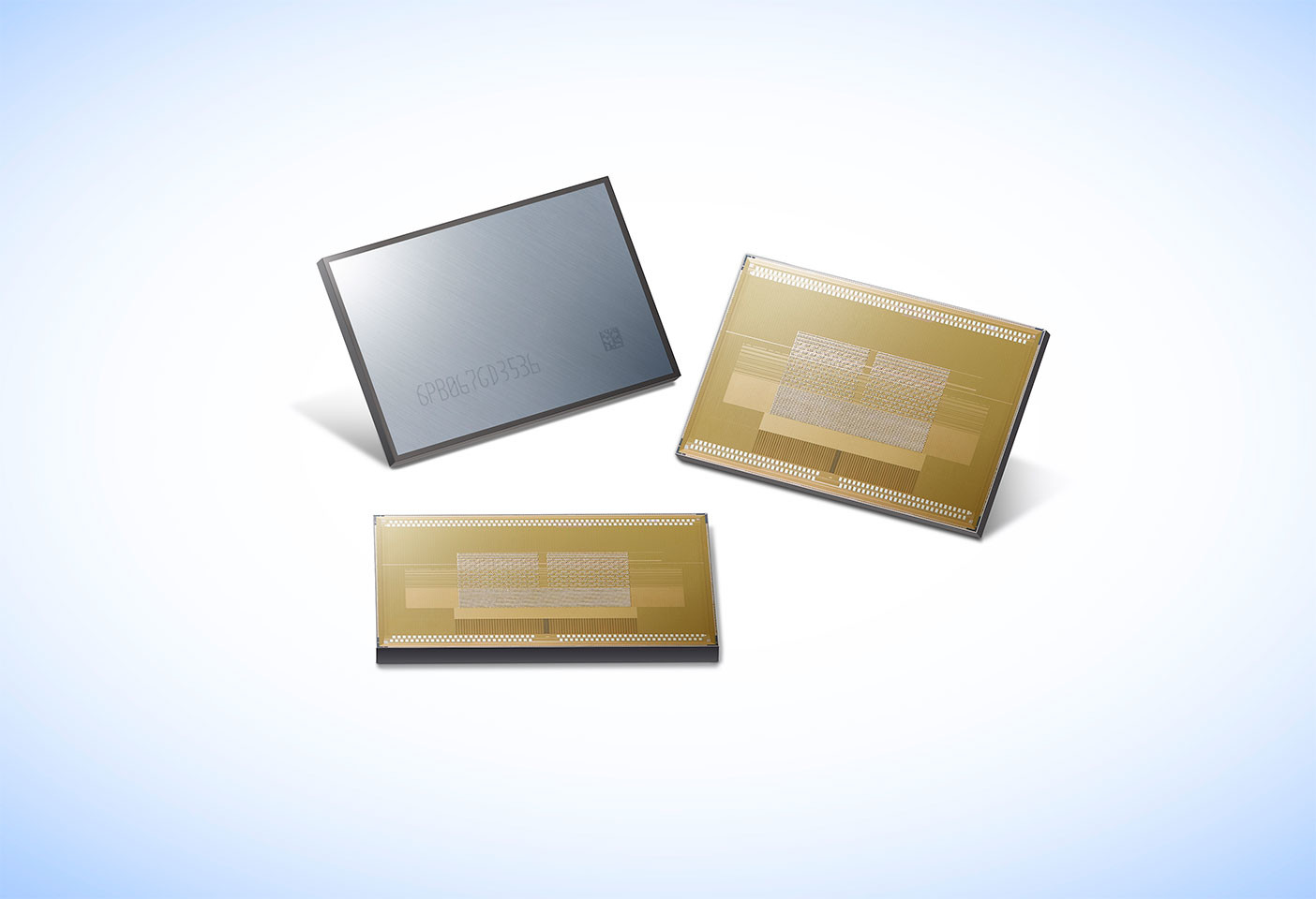
It seems our wait for custom editions of AMD's RX Vega graphics cards is coming to an end. "Better late than never" is what they always say; however, AMD and its AIB partners have to know that this kind of wait can sap customer enthusiasm for a product. It's not enough that customers waited around two years for Vega to come to fruition; we've also had to wait some additional months (not weeks), for an actual custom-design graphics card. Vega's exotic design with HBM2 memory means that these graphics cards' availability would fall prey not only to Vega GPU yields, but also to HBM2 memory availability.
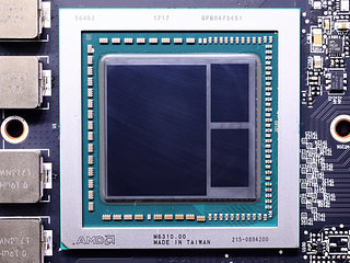
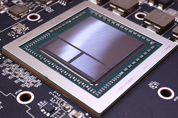
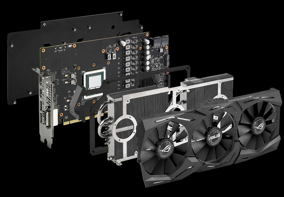
Additionally, Vega has been vulnerable to packaging of HBM2 and the GPU as well, with various factories providing different levels of quality in the finished product. This introduced some unexpected variance in the finished products - making the creation of cooling designs that could cope with all the design discrepancies more difficult.

Additionally, Vega has been vulnerable to packaging of HBM2 and the GPU as well, with various factories providing different levels of quality in the finished product. This introduced some unexpected variance in the finished products - making the creation of cooling designs that could cope with all the design discrepancies more difficult.