News Posts matching #HBM3

Return to Keyword Browsing

SK hynix Reports 2022 and Fourth Quarter Financial Results

SK hynix Inc. (or "the company") reported today financial results for 2022 ended on December 31. The company recorded revenues of 44.648 trillion won, an operating profit of 7.007 trillion won and a net income of 2.439 trillion won. Operating and net profit margin for the full year was 16% and 5%, respectively. "Revenues continued to grow last year, but the operating profit decreased compared with a year earlier as the industry entered into a downturn from the second half," the company said. "With uncertainties still lingering, we will continue to reduce investments and costs, while trying to minimize the impact of the downturn by prioritizing markets with high growth potential."

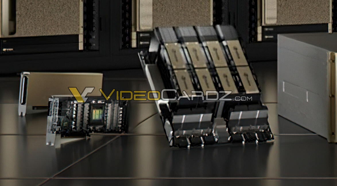
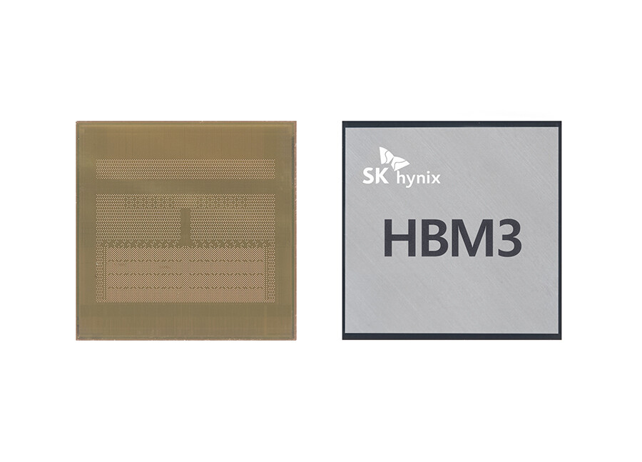
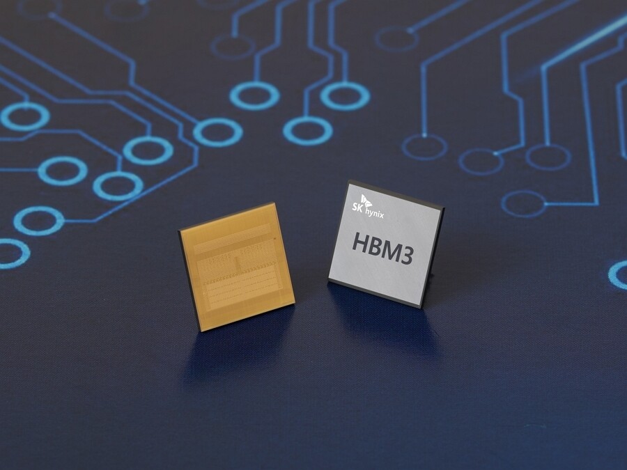
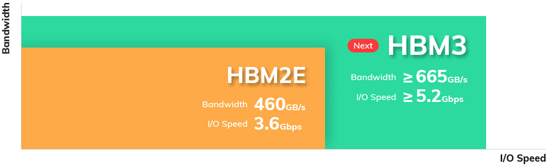
In 2022, SK hynix increased high-capacity DRAM shipments for server/PC markets, while boosting sales of DDR5 and HBM - of which products that the company has a solid market leadership - to customers in the growing markets of AI, Big Data, and cloud computing. Particularly, revenues for the data center SSD more than quadrupled compared with a year earlier.

AMD Shows Instinct MI300 Exascale APU with 146 Billion Transistors

During its CES 2023 keynote, AMD announced its latest Instinct MI300 APU, a first of its kind in the data center world. Combining the CPU, GPU, and memory elements into a single package eliminates latency imposed by long travel distances of data from CPU to memory and from CPU to GPU throughout the PCIe connector. In addition to solving some latency issues, less power is needed to move the data and provide greater efficiency. The Instinct MI300 features 24 Zen4 cores with simultaneous multi-threading enabled, CDNA3 GPU IP, and 128 GB of HBM3 memory on a single package. The memory bus is 8192-bit wide, providing unified memory access for CPU and GPU cores. CLX 3.0 is also supported, making cache-coherent interconnecting a reality.

The Instinct MI300 APU package is an engineering marvel of its own, with advanced chiplet techniques used. AMD managed to do 3D stacking and has nine 5 nm logic chiplets that are 3D stacked on top of four 6 nm chiplets with HBM surrounding it. All of this makes the transistor count go up to 146 billion, representing the sheer complexity of a such design. For performance figures, AMD provided a comparison to Instinct MI250X GPU. In raw AI performance, the MI300 features an 8x improvement over MI250X, while the performance-per-watt is "reduced" to a 5x increase. While we do not know what benchmark applications were used, there is a probability that some standard benchmarks like MLPerf were used. For availability, AMD targets the end of 2023, when the "El Capitan" exascale supercomputer will arrive using these Instinct MI300 APU accelerators. Pricing is unknown and will be unveiled to enterprise customers first around launch.

SK hynix to Showcase Energy-Efficient, High-Performance Memory Products at CES 2023

SK hynix Inc. announced today that it will showcase a number of its core and brand-new products at the CES 2023, the most influential tech event in the world taking place in Las Vegas from Jan. 5th through Jan. 8th. The products, introduced under the theme of the "Green Digital Solution," as part of the SK Group's "Carbon-Free Future" campaign, are expected to attract Big Tech customers and experts given the significant improvement in performance and energy efficiency compared with the previous generation as well as the effect of lessening the impact on the environment.

Attention on energy-efficient memory chips has been on the rise as global tech companies pursue products that process data faster, while consuming less energy. SK hynix is confident that its products to be displayed at the CES 2023 will meet customers' such needs with outstanding performance per watt and performance. The core product put forward at the show is PS1010 E3.S, an eSSD product composed of multiple 176-layer 4D NAND that supports the fifth generation of the PCIe interface.

SK hynix Reports Third Quarter 2022 Results

SK hynix Inc. reported today revenues of 10.98 trillion won, operating profit of 1.66 trillion won (with OP margin of 15%), and net income of 1.1 trillion won (with net income margin 10%) in the third quarter of 2022. Sales and operating profits decreased 20.5%, 60.5% respectively QoQ. SK hynix analyzed that revenues fell QoQ as both sales volume and price decreased due to sluggish demand for DRAM and NAND products amid worsening macroeconomic environment worldwide. In addition, SK hynix explained that despite the company improved cost competitiveness by increasing the sales proportion and yield of the latest 1anm DRAM and 176-layer 4D NAND, operating profit also decreased due to greater price drop than cost reduction.

SK hynix diagnosed that the semiconductor memory industry is facing an unprecedented deterioration in market conditions as uncertainties in the business environment continued. The deterioration occurred as the shipments of PCs and smartphone manufacturers, which are major buyers of memory chips, have decreased.

NVIDIA Could Launch Hopper H100 PCIe GPU with 120 GB Memory

NVIDIA's high-performance computing hardware stack is now equipped with the top-of-the-line Hopper H100 GPU. It features 16896 or 14592 CUDA cores, developing if it comes in SXM5 of PCIe variant, with the former being more powerful. Both variants come with a 5120-bit interface, with the SXM5 version using HBM3 memory running at 3.0 Gbps speed and the PCIe version using HBM2E memory running at 2.0 Gbps. Both versions use the same capacity capped at 80 GBs. However, that could soon change with the latest rumor suggesting that NVIDIA could be preparing a PCIe version of Hopper H100 GPU with 120 GBs of an unknown type of memory installed.

According to the Chinese website "s-ss.cc" the 120 GB variant of the H100 PCIe card will feature an entire GH100 chip with everything unlocked. As the site suggests, this version will improve memory capacity and performance over the regular H100 PCIe SKU. With HPC workloads increasing in size and complexity, more significant memory allocation is needed for better performance. With the recent advances in Large Language Models (LLMs), AI workloads use trillions of parameters for tranining, most of which is done on GPUs like NVIDIA H100.

NVIDIA Hopper Features "SM-to-SM" Comms Within GPC That Minimize Cache Roundtrips and Boost Multi-Instance Performance

NVIDIA in its HotChips 34 presentation revealed a defining feature of its "Hopper" compute architecture that works to increase parallelism and help the H100 processor better perform in a multi-instance environment. The hardware component hierarchy of "Hopper" is typical of NVIDIA architectures, with GPCs, SMs, and CUDA cores forming a hierarchy. The company is introducing a new component it calls "SM to SM Network." This is a high-bandwidth communications fabric inside the Graphics Processing Cluster (GPC), which facilitates direct communication among the SMs without making round-trips to the cache or memory hierarchy, play a significant role in NVIDIA's overarching claim of "6x throughput gain over the A100."

Direct SM-to-SM communication not just impacts latency, but also unburdens the L2 cache, letting NVIDIA's memory-management free up the cache of "cooler" (infrequently accessed) data. CUDA sees every GPU as a "grid," every GPC as a "Cluster," every SM as a "thread block," and every lane of SIMD units as a "lane." Each lane has a 64 KB of shared memory, which makes up 256 KB of shared local storage per SM as there are four lanes. The GPCs interface with 50 MB of L2 cache, which is the last-level on-die cache before the 80 GB of HBM3 serves as main memory.

SK hynix to Supply Industry's First HBM3 DRAM to NVIDIA

SK hynix announced that it began mass production of HBM3, the world's best-performing DRAM. The announcement comes just seven months after the company became the first in the industry to develop HBM3 in October, and is expected to solidify the company's leadership in the premium DRAM market. With accelerating advancements in cutting-edge technologies such as artificial intelligence and big data, major global tech companies are seeking ways to quickly process rapidly increasing volumes of data. HBM, with significant competitiveness in data processing speed and performance compared with traditional DRAM, is expected to draw broad industry attention and see rising adoption.

NVIDIA has recently completed its performance evaluation of SK hynix's HBM3 samples. SK hynix will provide HBM3 for NVIDIA systems expected to ship starting in the third quarter of this year. SK hynix will expand HBM3 volume in the first half in accordance with NVIDIA's schedule. The highly anticipated NVIDIA H100 is the world's largest and most powerful accelerator. SK hynix's HBM3 is expected to enhance accelerated computing performance with up to 819 GB/s of memory bandwidth, equivalent to the transmission of 163 FHD (Full-HD) movies (5 GB standard) every second.

NVIDIA H100 SXM Hopper GPU Pictured Up Close

ServeTheHome, a tech media outlet focused on everything server/enterprise, posted an exclusive set of photos of NVIDIA's latest H100 "Hopper" accelerator. Being the fastest GPU NVIDIA ever created, H100 is made on TSMC's 4 nm manufacturing process and features over 80 billion transistors on an 814 mm² CoWoS package designed by TSMC. Complementing the massive die, we have 80 GB of HBM3 memory that sits close to the die. Pictured below, we have an SXM5 H100 module packed with VRM and power regulation. Given that the rated TDP for this GPU is 700 Watts, power regulation is a serious concern and NVIDIA managed to keep it in check.

On the back of the card, we see one short and one longer mezzanine connector that acts as a power delivery connector, different from the previous A100 GPU layout. This board model is labeled PG520 and is very close to the official renders that NVIDIA supplied us with on launch day.

NVIDIA Hopper Whitepaper Reveals Key Specs of Monstrous Compute Processor

The NVIDIA GH100 silicon powering the next-generation NVIDIA H100 compute processor is a monstrosity on paper, with an NVIDIA whitepaper published over the weekend revealing its key specifications. NVIDIA is tapping into the most advanced silicon fabrication node currently available from TSMC to build the compute die, which is TSMC N4 (4 nm-class EUV). The H100 features a monolithic silicon surrounded by up to six on-package HBM3 stacks.

The GH100 compute die is built on the 4 nm EUV process, and has a monstrous transistor-count of 80 billion, a nearly 50% increase over the GA100. Interestingly though, at 814 mm², the die-area of the GH100 is less than that of the GA100, with its 826 mm² die built on the 7 nm DUV (TSMC N7) node, all thanks to the transistor-density gains of the 4 nm node over the 7 nm one.

AMD MI300 Compute Accelerator Allegedly Features Eight Logic Dies

AMD's next-generation MI300 compute accelerator is expected to significantly scale up the logic density, according to a rumor by Moore's Law is Dead. Based on the CDNA3 compute architecture, the MI300 will be a monstrous large multi-chip module with as many as 8 logic dies (compute dies), each with its dedicated HBM3 stack. The compute dies (logic dies), will be 3D-stacked on top of I/O dies that pack the memory controllers, and the interconnect that performs the inter-die, and inter-package communication.

The report even goes on to mention that the compute die at the top level of the stack will be built on TSMC N5 (5 nm) silicon fabrication process, while the I/O die below will be TSMC N6 (6 nm). At this point it's not known if AMD will use the package to wire the logic stacks to the memory stacks, or whether it will take the pricier route of using a silicon interposer, but the report supports the interposer theory—that an all-encompassing interposer seats all eight compute dies, all four I/O dies (each with two compute dies), and the eight HBM3 stacks. An interposer is a silicon die that facilitates high density microscopic wiring between two dies on a package, which are otherwise not possible through large package substrate wiring.

SK Hynix Presents HBM3 DRAM at NVIDIA GTC 2022

SK hynix, was the only company that presented its HBM3, a high-end product known as the fastest DRAM in existence with the biggest capacity, at NVIDIA GTC (GPU Technology Conference) 2022, which took place on March 21~24. Known as the world's best-performing DRAM, HBM3 is the fourth generation of the HBM (High Bandwidth Memory) technology. SK hynix's HBM3 uses over 8,000 TSVs per stack (i.e. over 100,000 TSVs in a 12-Hi stack) and can feature up to 12-Hi stack, which is an upgrade from the previous HBM2E's 8-Hi stack. When fully stacked, it can offer up to 24 GB of capacity. With a 16-channel architecture, it runs at 6.4 Gbps, which is double that of HBM2E and which is the fastest in the world, expecting to further accelerate our digital life.

For instance, HBM has become a prerequisite for the Levels 4 and 5 of driving automation when it comes to autonomous vehicles, a topic that has garnered a great deal of attention nowadays. Also, HBM3 is expected to play an even bigger role along with the growth of High Performance Computing (HPC), Artificial Intelligence (AI), Machine Learning (ML), and Advanced Driver Assistance Systems (ADAS) markets fueled by the acceleration of digital transformation.

NVIDIA Announces Hopper Architecture, the Next Generation of Accelerated Computing

GTC—To power the next wave of AI data centers, NVIDIA today announced its next-generation accelerated computing platform with NVIDIA Hopper architecture, delivering an order of magnitude performance leap over its predecessor. Named for Grace Hopper, a pioneering U.S. computer scientist, the new architecture succeeds the NVIDIA Ampere architecture, launched two years ago.

The company also announced its first Hopper-based GPU, the NVIDIA H100, packed with 80 billion transistors. The world's largest and most powerful accelerator, the H100 has groundbreaking features such as a revolutionary Transformer Engine and a highly scalable NVIDIA NVLink interconnect for advancing gigantic AI language models, deep recommender systems, genomics and complex digital twins.

First Pictures of NVIDIA "Hopper" H100 Compute Processor Surface

Here's the first picture of an NVIDIA H100 "Hopper" compute processor, which succeeds the two-year old "Ampere" A100. The "Hopper" compute architecture doubles down on the strengths of "Ampere," in having the most advanced AI deep-learning compute machinery, FP64 math capability, and lots more. Built on the TSMC N5 (5 nm) node, the "GH100" processor more than doubles the transistor-count over the A100, which is expected to be around 140 billion.

Unlike the A100, the H100 will come with graphics rendering capability, The GH100 is one of the first NVIDIA chips to feature two different kinds of GPCs. Of the six GPCs has NVIDIA's graphics-relevant SMs, whereas the other GPCs have compute-relevant SMs. The graphics SM will have components such as RT cores, and other raster machinery; while the compute SMs will have specialized tensor cores and FP64 SIMD units. Counting the graphics SM, there are a total of 144 SMs on the silicon. Memory is care of what could be a 6144-bit HBM3 interface. NVIDIA will build various products based on the "GH100," including SXM cards, DGX Stations, SuperPods, and even PCIe add-in cards (AICs). NVIDIA is expected to unveil the H100 later today.

SK hynix Reports Fiscal Year 2021 and Fourth Quarter Results

SK hynix today announced financial results for its fiscal year 2021 ended on December 31, 2021. The consolidated revenue of fiscal year 2021 was 42.998 trillion won, while the operating profit amounted to 12.410 trillion won and the net income 9.616 trillion won. Operating margin for the year was 29% and net margin was 22%. SK hynix achieved record high annual revenue since its foundation. This surpasses the revenue in 2018 when the semiconductor market was in its biggest boom.

Despite uncertain market conditions such as supply chain disruptions, demand for contactless IT technology has increased. Based on its technology and quality competitiveness, SK hynix managed to supply its products proactively, achieving record-breaking annual sales. For DRAM, SK hynix focused on securing profitability by flexibly responding to demands in PC and server applications in DRAM business. Furthermore, by developing the industry's first DDR5 and HBM3 DRAM, SK hynix has secured leading quality competitiveness in high value-added next-gen products.

JEDEC Publishes HBM3 Update to High Bandwidth Memory (HBM) Standard

JEDEC Solid State Technology Association, the global leader in the development of standards for the microelectronics industry, today announced the publication of the next version of its High Bandwidth Memory (HBM) DRAM standard: JESD238 HBM3, available for download from the JEDEC website. HBM3 is an innovative approach to raising the data processing rate used in applications where higher bandwidth, lower power consumption and capacity per area are essential to a solution's market success, including graphics processing and high-performance computing and servers.

Samsung Talks DDR6-12800, GDDR7 Development, and HBM3 Volume Production

During Samsung's Tech Day 2021, the company presented some interesting insights about the future of system memory technologies and how it plans to execute its production. Starting with the latest DDR5 standard, the company intends to follow JEDEC documents and offer some overclocking modules that surpass the specification advised by JEDEC. While the DDR5 standard specifies memory modules with 6,400 MT/s, Samsung will develop modules capable of overclocking up to 8,400 MT/s. These are not yet confirmed as they are still in the development phase. However, we can expect to see them in the later life of DDR5 memory.

The company also talked about the DDR6 standard, which is supposedly twice as fast as DDR5. The new DDR6 standard is still in early development, and all we know so far is that the number of memory channels per module is seeing a twofold increase over DDR5 to four channels. The number of memory banks also increases to 64. In addition to DDR6 for desktop and server use cases, the company is also working on Low Power DDR6 (LPDDR6) for mobile applications. While the company's LPDDR5 memory goes into volume production using the 1a-nm process at the beginning of 2022, the LPDDR6 is still in early development. The base speed for DDR6 modules will allegedly arrive at 12,800 MT/s, while overclocking modules will join the party at up to 17,000 MT/s. Mobile-oriented LPDDR6 version is also supposed to come with up to 17,000 MT/s speeds.

SK hynix Announces Development of HBM3 DRAM

SK hynix Inc. announced that it has become the first in the industry to successfully develop the High Bandwidth Memory 3, the world's best-performing DRAM. HBM3, the fourth generation of the HBM technology with a combination of multiple DRAM chips vertically connected, is a high value product that innovatively raises the data processing rate.

The latest development, which follows the start of mass production of HBM2E in July last year, is expected to help consolidate the company's leadership in the market. SK hynix was also the first in the industry to start mass production of HBM2E. SK hynix's HBM3 is not only the fastest DRAM in the world, but also comes with the biggest capacity and significantly improved level of quality.

Synopsys Accelerates Multi-Die Designs with Industry's First Complete HBM3 IP and Verification Solutions

Synopsys, Inc. today announced the industry's first complete HBM3 IP solution, including controller, PHY, and verification IP for 2.5D multi-die package systems. HBM3 technology helps designers meet essential high-bandwidth and low-power memory requirements for system-on-chip (SoC) designs targeting high-performance computing, AI and graphics applications. Synopsys' DesignWare HBM3 Controller and PHY IP, built on silicon-proven HBM2E IP, leverage Synopsys' interposer expertise to provide a low-risk solution that enables high memory bandwidth at up to 921 GB/s.

The Synopsys verification solution, including Verification IP with built-in coverage and verification plans, off-the-shelf HBM3 memory models for ZeBu emulation, and HAPS prototyping system, accelerates verification from HBM3 IP to SoCs. To accelerate development of HBM3 system designs, Synopsys' 3DIC Compiler multi-die design platform provides a fully integrated architectural exploration, implementation and system-level analysis solution.

Samsung Brings In-memory Processing Power to Wider Range of Applications

Samsung Electronics the world leader in advanced memory technology, today showcased its latest advancements with processing-in-memory (PIM) technology at Hot Chips 33—a leading semiconductor conference where the most notable microprocessor and IC innovations are unveiled each year. Samsung's revelations include the first successful integration of its PIM-enabled High Bandwidth Memory (HBM-PIM) into a commercialized accelerator system, and broadened PIM applications to embrace DRAM modules and mobile memory, in accelerating the move toward the convergence of memory and logic.

In February, Samsung introduced the industry's first HBM-PIM (Aquabolt-XL), which incorporates the AI processing function into Samsung's HBM2 Aquabolt, to enhance high-speed data processing in supercomputers and AI applications. The HBM-PIM has since been tested in the Xilinx Virtex Ultrascale+ (Alveo) AI accelerator, where it delivered an almost 2.5X system performance gain as well as more than a 60% cut in energy consumption.

Rambus Innovates 8.4 Gbps HBM3-ready Memory Subsystem

Rambus Inc., a premier chip and silicon IP provider making data faster and safer, today announced the Rambus HBM3-ready memory interface subsystem consisting of a fully-integrated PHY and digital controller. Supporting breakthrough data rates of up to 8.4 Gbps, the solution can deliver over a terabyte per second of bandwidth, more than double that of high-end HBM2E memory subsystems. With a market-leading position in HBM2/2E memory interface deployments, Rambus is ideally suited to enable customers' implementations of accelerators using next-generation HBM3 memory.

"The memory bandwidth requirements of AI/ML training are insatiable with leading-edge training models now surpassing billions of parameters," said Soo Kyoum Kim, associate vice president, Memory Semiconductors at IDC. "The Rambus HBM3-ready memory subsystem raises the bar for performance enabling state-of-the-art AI/ML and HPC applications."

SK Hynix Details its Upcoming HBM3 Memory: 665 GB/s per Stack

SK Hynix is at the forefront of developing the next generation of stacked high-bandwidth memory, the HBM3 standard. Succeeding the current HBM2e standard, HBM3 will power next-generation HPC and AI processors in high-density multi-chip modules. A Tom's Hardware report citing information from SK Hynix reveals two key details about the new standard. For starters, it could offer per-pin data-rates of 5.2 Gbps, a 44% increase over the 3.6 Gbps that HBM2e caps out at. This results in a per-stack bandwidth of 665 GB/s, compared to 480 GB/s for the HBM2e. A processor with four such stacks (over a 4096-bit wide bus), would hence enjoy 2.66 TB/s of memory bandwidth. It's likely that HBM3 stacks from SK Hynix could implement the DBI Ultra 2.5D/3D hybrid bonding interconnect technology licensed from Xperi Corp.

OpenFive Tapes Out SoC for Advanced HPC/AI Solutions on TSMC 5 nm Technology

OpenFive, a leading provider of customizable, silicon-focused solutions with differentiated IP, today announced the successful tape out of a high-performance SoC on TSMC's N5 process, with integrated IP solutions targeted for cutting edge High Performance Computing (HPC)/AI, networking, and storage solutions.

The SoC features an OpenFive High Bandwidth Memory (HBM3) IP subsystem and D2D I/Os, as well as a SiFive E76 32-bit CPU core. The HBM3 interface supports 7.2 Gbps speeds allowing high throughput memories to feed domain-specific accelerators in compute-intensive applications including HPC, AI, Networking, and Storage. OpenFive's low-power, low-latency, and highly scalable D2D interface technology allows for expanding compute performance by connecting multiple dice together using an organic substrate or a silicon interposer in a 2.5D package.

Intel Xe HPC Multi-Chip Module Pictured

Intel SVP for architecture, graphics, and software, Raja Koduri, tweeted the first picture of the Xe HPC scalar compute processor multi-chip module, with its large IHS off. It reveals two large main logic dies built on the 7 nm silicon fabrication process from a third-party foundry. The Xe HPC processor will be targeted at supercomputing and AI-ML applications, so the main logic dies are expected to be large arrays of execution units, spread across what appear to be eight clusters, surrounded by ancillary components such as memory controllers and interconnect PHYs.

There appear to be two kinds of on-package memory on the Xe HPC. The first kind is HBM stacks (from either the HBM2E or HBM3 generation), serving as the main high-speed memory; while the other is a mystery for now. This could either be another class of DRAM, serving a serial processing component on the main logic die; or a non-volatile memory, such as 3D XPoint or NAND flash (likely the former), providing fast persistent storage close to the main logic dies. There appear to be four HBM-class stacks per logic die (so 4096-bit per die and 8192-bit per package), and one die of this secondary memory per logic die.

Micron Also Announces Development of HBMnext

Continuing from the Micron tech brief we shared earlier, a new interesting prospect for the future of ultra-bandwidth solutions is being called simply HBMnext. It's very likely this is only a working title for a next generation HBM memory interface, whether it is a mere evolution of HBM2E or HBM3 proper. The jump in memory speed from HBM2E to HBMnext is still under wraps; however, we've seen HBM2E take significant strides compared to HBM2 already. The first HBM2E products arrived with a 0.4 Gbps improvement over HBM2 (2.4 Gbps vs 2.0 Gbps), but HBM2E has already been certified - and is announced by Micron - as hitting 3.2 Gbps as soon as the second half of this year. One can expect HBMnext to take somewhat comparable strides. Users shouldn't expect to see HBMnext on any products soon, though; it's only expected to launch come 2022.

Samsung Now Mass Producing Industry's First 2nd-Generation 10nm Class DRAM

Samsung Electronics Co., Ltd., the world leader in advanced memory technology, announced today that it has begun mass producing the industry's first 2nd-generation of 10-nanometer class (1y-nm), 8-gigabit (Gb) DDR4 DRAM. For use in a wide range of next-generation computing systems, the new 8 Gb DDR4 features the highest performance and energy efficiency for an 8 Gb DRAM chip, as well as the smallest dimensions.

"By developing innovative technologies in DRAM circuit design and process, we have broken through what has been a major barrier for DRAM scalability," said Gyoyoung Jin, president of Memory Business at Samsung Electronics. "Through a rapid ramp-up of the 2nd-generation 10 nm-class DRAM, we will expand our overall 10 nm-class DRAM production more aggressively, in order to accommodate strong market demand and continue to strengthen our business competitiveness."
Return to Keyword Browsing
May 15th, 2024 18:13 EDT change timezone

New Forum Posts

Popular Reviews

Controversial News Posts