News Posts matching #Hynix

Return to Keyword Browsing

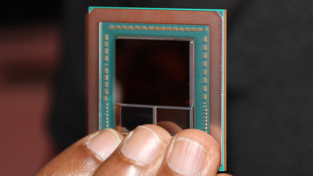
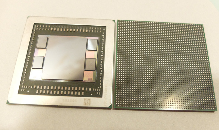
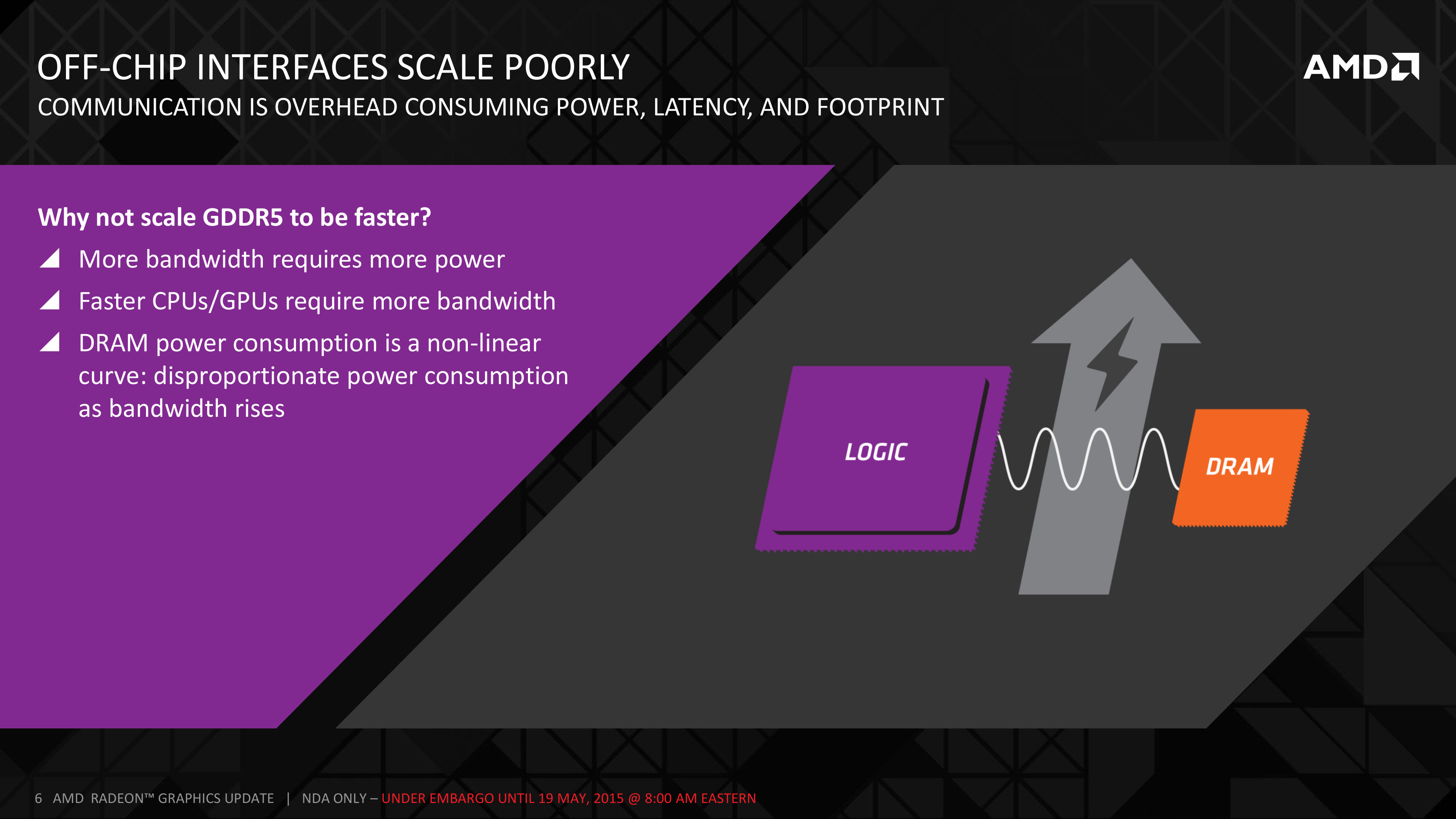
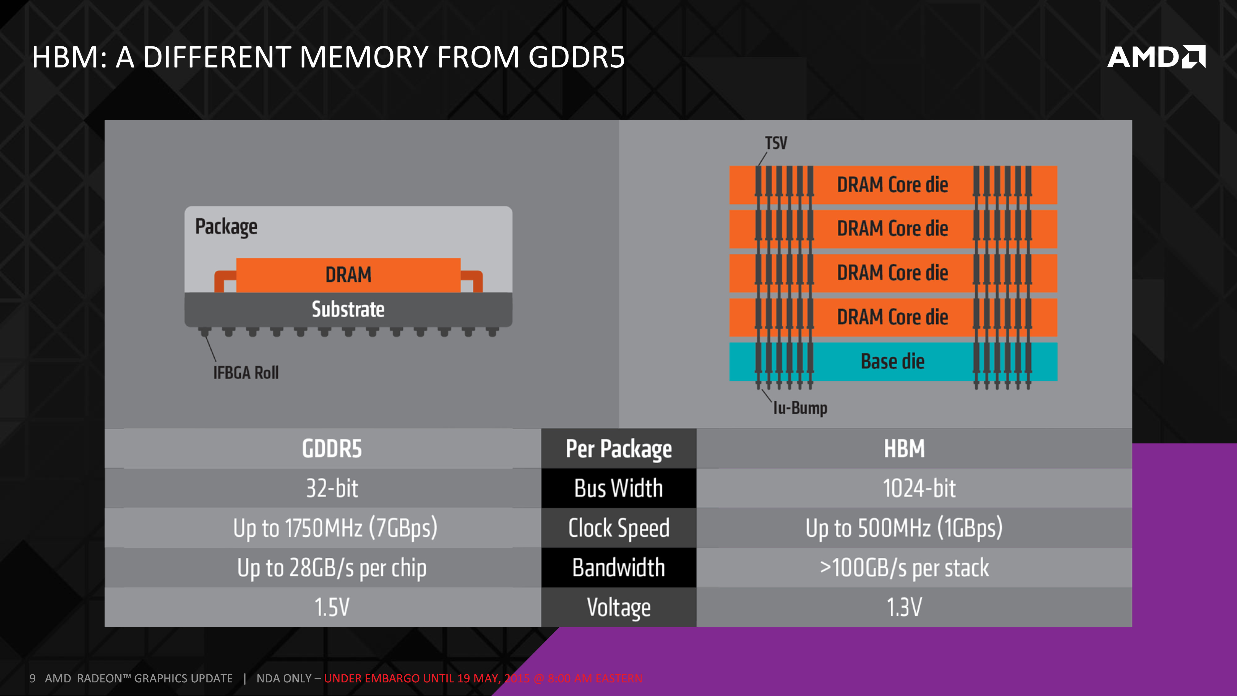
SK Hynix 4 Gigabyte HBM2 Stack Availability Paves the way for Vega

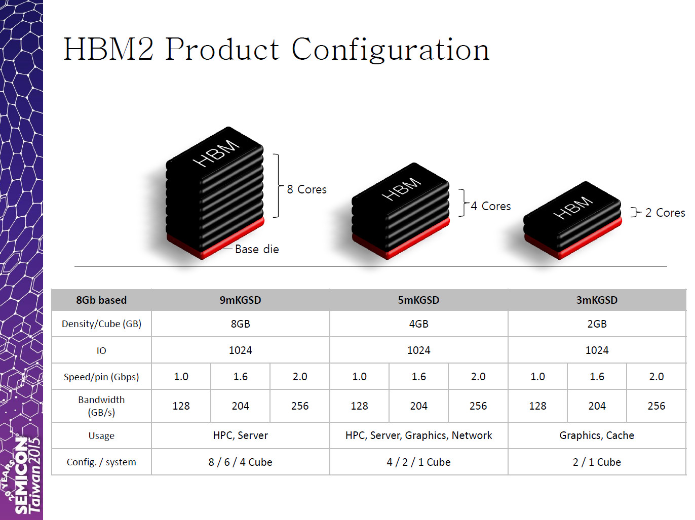
SK Hynix, the principal supplier of high bandwidth memory (HBM) stacks to AMD since its pioneering Radeon R9 Fury series, released an updated HBM2 specifications document that pins availability of 4 gigabyte (32 Gbit) HBM2 stacks to the first quarter of 2017. This paves the way for mass-production and market availability of AMD's upcoming Radeon "Vega" graphics chip, which feature two such 4 GB HBM2 stacks, making up 8 GB of total memory.

SK Hynix H5VR32ESM4H-H1K memory stack, which will be integrated by AMD onto its Vega10 multi-chip module (MCM), ticks at 1.60 Gbps (per pin), with a cumulative bandwidth of 204.8 GB/s per stack. With two such stacks, Vega10 could feature 409.6 GB/s of memory bandwidth, assuming AMD uses the reference clock speeds for these stacks.

SK Hynix to Construct a Cutting Edge NAND Flash FAB in Cheongju

SK Hynix Inc. announced it will construct a new memory semiconductor FAB in Cheongju, Chungcheongbuk-do to meet increasing NAND Flash demand. This is a part of a mid/long-term investment plan that SK Hynix declared at M14 completion ceremony in August 2015. At that time, the Company said it could spend 46 trillion won to set up 3 new FABs in Icheon and Cheongju including the M14.

The new FAB will be located in a Cheongju Technopolis site. SK Hynix starts a design within next month then begins construction of the shell and the cleanroom in August 2017 to be completed in June 2019 with total investment of 2.2 trillion won. Equipment installation into the FAB shall be decided considering market conditions as well as the Company's migration plans.

Plextor Extends EX1 Portable SSD Warranty

Plextor today announced that it revised the warranty policy of its recently announced EX1 portable solid-state drive to be effective for 5 years, from its existing 3 years. This change is applicable to all products already sold and with retailers as unsold inventory. The EX1 is a series of portable SSDs with 10 Gb/s USB 3.1 host interface, with a single cable handling both power and host connectivity. The drives combine Silicon Motion-made controllers with SK Hynix 16 nm TLC NAND flash memory, and come in capacities of 128 GB, 256 GB, 512 GB, priced at 79€, 119€, and 213€, respectively.

Plextor Announces the EX 1 External SSD Drive

The specialist for high-performance digital memory technology and Solid State Drive products (SSD), Plextor, presents its new generation of ultra-light, small form factor, high-speed external SSD with OTG support and only 30g in weight: the Plextor EX1. The Plextor EX1 specifications are designed for high speeds, with the USB Type-C interface supporting USB 3.1 Gen2 standard, and delivering a 10x higher speed compared to the USB 2.0 interface, delivering continuous read/write speeds of 550 and 500 MB/s respectively.

The strength of the EX1 series is based on the core components used, including high-quality TLC NAND flash memory manufactured using Hynix's 16nm process, as well as the latest generation of controller ICs from SMI. Plextor has also developed an advanced firmware, and includes the PlexNitro application for increased user control. The Plextor EX1 will be available in stores from the end of November in three different storage capacities with 128GB, 256GB and 512GB. The EX1 complies with Plextor's stringent quality requirements, including a 3-year warrant. Pricing will be announced at a later date.

Third-Generation HBM Could Enable Graphics Cards with 64GB Memory

One of the first drafts of the HBM3 specification reveals that the standard could enable graphics cards with up to 64 GB of video memory. The HBM2 memory, which is yet to make its consumer graphics debut, caps out at 32 GB, and the first-generation HBM, which released with the AMD Radeon Fury series, at just 4 GB.

What's more, HBM3 doubles bandwidth over HBM2, pushing up to 512 GB/s per stack. A 4096-bit HBM3 equipped GPU could have up to 2 TB/s (yes, terabytes per second) of memory bandwidth at its disposal. SK Hynix, one of the key proponents of the HBM standard, even claims that HBM3 will be both more energy-efficient and cost-effective than existing memory standards, for the performance on offer. Some of the first HBM3 implementations could come from the HPC industry, with consumer implementations including game consoles, graphics cards, TVs, etc., following later.

SK Hynix to Ship HBM2 Memory by Q3-2016

Korean memory and NAND flash giant SK Hynix announced that it will have HBM2 memory ready for order within Q3-2016 (July-September). The company will ship 4 gigabyte HBM2 stacks in the 4 Hi-stack (4-die stack) form-factor, in two speeds - 2.00 Gbps (256 GB/s per stack), bearing model number H5VR32ESM4H-20C; and 1.60 Gbps (204 GB/s per stack), bearing model number H5VR32ESM4H-12C. With four such stacks, graphics cards over a 4096-bit HBM2 interface, graphics cards with 16 GB of total memory can be built.

SK Hynix to Ship 4GB HBM2 Stacks by Q3-2016

Korean DRAM and NAND flash giant SK Hynix will be ready to ship its 4 GB stacked second generation high-bandwidth memory (HBM2) chips from Q3, 2016. These packages will be made up of four 1 GB dies, with a bandwidth-per-pin of 1 Gbps, 1.6 Gbps, and 2 Gbps, working out to per-stack bandwidths of 128 GB/s, 204 GB/s, and 256 GB/s, respectively.

These chips will target applications such as graphics cards, network infrastructure, HPC, and servers. The company is also designing 8 GB stacks, made up of eight 1 GB dies. These stacks will be targeted at HPC and server applications. The company is also offering cost-effective 2 GB, 2-die stacks, for graphics cards. The cost-effective 2 GB, 2-die stacks could prove particularly important for the standard's competition against GDDR5X, particularly in mid-range and performance-segment graphics cards.

AMD Showcases Graphics, Energy Efficient Computing and Die-Stacking Innovation

Top technologists from AMD are detailing the engineering accomplishments behind the performance and energy efficiency of the new high-performance Accelerated Processing Unit (APU), codenamed "Carrizo," and the new AMD Radeon R9 Fury family of GPUs, codenamed "Fiji," at the prestigious annual Hot Chips symposium starting today. The presentations will focus on new details of the high-definition video and graphics processing engines on the 6th Generation AMD A-Series APU ("Carrizo"), and the eight year journey leading to die-stacking technology and all-new memory architecture included on the latest top-of-the-line AMD Radeon Fury Series GPUs ("Fiji") for 4K gaming and VR. Using a true System-on-Chip (SoC) design, 6th Generation AMD A-Series processors are designed to reduce the power consumed by the x86 cores alone by 40 percent, while providing substantial gains in CPU, graphics, and multimedia performance versus the prior generation APU. The new AMD Radeon R9 Fury X GPU achieves up to 1.5x the performance-per-watt of the previous high-end GPU from AMD.

"With our new generation of APU and GPU technology, our engineering teams left no stone unturned for performance and energy efficiency," said Mark Papermaster, chief technology officer at AMD. "Using innovative design for our APUs, we've vastly increased the number of transistors on-chip to increase functionality and performance, implemented advanced power management, and completed the hardware implementation of Heterogeneous System Architecture. For our latest GPUs, AMD is the first to introduce breakthrough technology in the form of die-stacking and High-Bandwidth Memory. The results are great products with very large generational performance-per-watt gains."

SanDisk and SK Hynix Settle IP Litigation

SanDisk Corporation, a global leader in flash storage solutions, today announced it has reached agreement with SK Hynix, Inc. to modify and extend their intellectual property licensing relationship and enter into a multi-year commercial relationship under which SK Hynix will supply its leading-edge DRAM products to SanDisk. These agreements include a settlement of the trade secret misappropriation suit filed by SanDisk in 2014.

Under these agreements, which will expire on March 31, 2023, SanDisk will release SK Hynix of its liability pertaining to the trade secret litigation and license certain intellectual property rights to SK Hynix in exchange for license and royalty payments to be made over the duration of the agreement. In addition, SK Hynix has agreed to supply SanDisk with certain volumes of its DRAM products for MCP and SSD applications. The specific terms and conditions of the agreements, including with respect to economic consideration, are confidential.

SK Hynix Launches In-house UFS 2.0 Solution

SK Hynix Inc. announced it has developed UFS (Universal Flash Storage) 2.0 64 GB (Gigabytes) solution based on its own 16 nm NAND Flash and in-house firmware and controller. This UFS 2.0 represents a groundbreaking leap in performance by enabling High-Speed Gear 3 interface with dual data lanes.

UFS 2.0 is the next generation of embedded flash memory to eMMC for mobile IT gadgets which drives a remarkable boost in reading/writing speed at low power and supports high density. The Company's UFS 2.0 operates at 780 MB/s(Megabytes per second) and 160 MB/s of sequential read/write speed and runs random read/write speed at 32,000 IOPS and 17,000 IOPS. As a result, it works three times faster in read speed than eMMC 5.1.

In addition, this UFS 2.0 utilizes 'Command Queue' technology used in SSD solutions to handle read and write commands simultaneously to achieve data operation efficiency by preventing buffering load in multi-tasking and ordering priorities of data works. To maximize prioritized command processing feature of UFS standard, the device employs 'Multi-Thread' read processing internally to ensure that high priority command is serviced first irrespective of other outstanding tasks, delivering fast response to time-critical host requests for best user experience. In consequence, it realizes even better performance in speed and power consumption over eMMC.

Micron Begins Shipping its First 20 nm-class GDDR5 DRAM Chips

Micron Technology announced during its Q3 FY-2015 earnings call, that it began shipping GDDR5 memory chips based on its 20 nm-class node. The company is reportedly shipping 8 Gb (1 gigabyte) GDDR5 memory chips. The company was last reported to be acquiring Japanese DRAM major Elpida, which also supplies GDDR5 chips to graphics cards, notebooks, and game console makers. The GDDR5 memory space has been saturated by companies such as Samsung and SK Hynix. The memory standard itself is on the brink of becoming obsolete; with AMD implementing HBM on its new high-end GPU, and NVIDIA expected to implement HBM with its upcoming "Pascal" GPU family. There is still quite a few GDDR5-equipped graphics cards to be sold, before HBM takes over GPUs of all market segments.

KLEVV High Performance Gaming Memory Modules Now Available in Europe

Essencore Limited, a noteworthy newcomer in DRAM modules and NAND Flash application products including Gaming Memory Modules, Solid State Drives, USB Flash Drives and MicroSD cards, is pleased to announce the sales kick-off in European countries with its brand "KLEVV". In attempt to expand its global presence and to accelerate growth, Essencore hopes that this KLEVV product launch will help to efficiently deliver its premium products to its European customer.

As a young company founded in 2014 by CEO IU Kim, Essencore strives to become world's leading vendor of both DRAM modules and NAND Flash application products. To achieve this goal, Essencore has introduced its house brand "KLEVV" with the industry's first-rate quality and best performing products. In a conscious move to strengthen brand awareness and products at this early stage, KLEVV will focus on the three key consumer markets of U.S., Europe and China. Of all regions, Europe is deemed to have the highest potential, with its huge population of tech enthusiasts. Starting in Germany, UK, and Poland in summer 2015, KLEVV products will soon be available in all corners of Europe.

AMD "Fiji" HBM Implementation Detailed

Back in 2008, when it looked like NVIDIA owned the GPU market, and AMD seemed lagging behind on the performance and efficiency game, the company sprung a surprise. The company's RV770 silicon, the first GPU to implement GDDR5 memory, trounced NVIDIA's big and inefficient GeForce GTX 200 series, and threw AMD back in the game. GDDR5 helped the company double the memory bandwidth, with lower pin- and memory-chip counts, letting the company and its partners build graphics cards with fewer components, and earn great margins, which the company invested in development of its even better HD 5000 series, that pushed NVIDIA with its comical GeForce GTX 480, to hit its lowest ever in market-share. Could AMD be looking at a similar turnaround this summer?

Since the introduction of its Graphics CoreNext architecture in 2012, AMD has been rather laxed in its product development cycle. The company has come out with a new high-end silicon every 18-24 months, and adopted a strategy of cascading re-branding. The introduction of each new high-end silicon would relegate the existing high-end silicon to the performance segment re-branded, and the existing performance-segment silicon to mid-range, re-branded. While the company could lay out its upcoming Radeon R9 series much in the same way, with the introduction of essentially just one new silicon, "Fiji," it could just prove enough for the company. Much like RV770, "Fiji" is about to bring something that could prove to be a very big feature to the consumer graphics market, stacked high-bandwidth memory (HBM).

LiteOn Intros ZETA Series Consumer SSDs

An OEM for notable SSD brands such as Plextor, LiteOn kicked off its own consumer SSD line, with ZETA. Built in the 7 mm thick, 2.5-inch form-factor, with SATA 6 Gb/s interface, these drives come in three capacities, 128 GB (LCH-128V2S), 256 GB (LCH-256V2S), and 512 GB (LCH-512V2S), featuring LPDDR3 controller cache of 128 MB, 256 MB, and 512 MB, respectively. The drive is based on Silicon Motion SM2246EN controller, with 16 nm MLC NAND flash, made by SK Hynix.

All three capacities offer sequential read speeds of up to 520 MB/s, differing with sequential write speeds. The 128 GB variant offers up to 150 MB/s writes, the 256 GB variant offers up to 260 MB/s, and the 512 GB variant up to 430 MB/s. Their 4K random-access read speeds are up to 67,500 IOPS, up to 82,500 IOPS, and up to 83,500 IOPS, respectively; and random-access write speeds are up to 37,500 IOPS, up to 72,500 IOPS, and up to 80,000 IOPS, respectively. Most common client SSD features, such as TRIM, NCQ, and 256-bit AES native encryption, are part of the package. LiteOn didn't announce pricing information for markets outside the Greater China region, where the drives will make their debut.

Century Micro Launches First Low-profile DDR4 DIMM

Japanese company Century Micro launched the world's first low-profile (half-height) DDR4 DIMM (model: CK4GX4-D4RE2133VL81). With a module height of just 1.87 cm, the 4 GB module uses DRAM chips made by SK Hynix, and offers JEDEC-specified DDR4-2133 MHz speeds, with 15-15-15 timings, and 1.2V DRAM voltage. It sells in 16 GB kits of four modules, which sells at 51,980 JPY (US $428), including taxes.

SK Hynix Developed the World's Highest Density 16 GB NVDIMM

SK Hynix Inc. announced that it has developed the world's highest density 16 GB (Gigabytes) of NVDIMM (Non Volatile DIMM) based on 4 Gb (Gigabit) DDR4 using its advanced 20 nm class technology.

This NVDIMM is able to send DRAM data to NAND Flash whose density is two times bigger than the DRAM in a unanticipated power loss by combining DRAM, NAND Flash and the module controller in a single module. Therefore, it is feasible to save and restore data safely as well as performing on the same level with general DDR4 modules. This new product works at 2133 Mbps and with a 64-bit I/O it processes up to 17 GB of data per second running at 1.2V.

ADATA Premier DDR4 Memory Modules Spotted in Stores

Wanna build a Haswell-E HEDT build on the "cheap?" Then this could make it to your list. ADATA is ready with its no-frills Premier line of DDR4 memory modules, which are sold in single-module packs of 4 GB and 8 GB. The modules stick to JEDEC specifications of DDR4-2133 MHz (PC4-17000), with CAS latencies of 15T, and voltage of 1.2 Volt. The modules use DRAM chips made by SK Hynix. Inclusive of all taxes, the 4 GB module is priced at the equivalent of $75 USD in Japan; and the 8 GB module goes for the equivalent of $150.

NAND Flash Brand Supplier Revenue Falls 6.6% in First Quarter

The shipment performances of Smartphones, Tablets, and Notebooks were relatively weak in the first quarter due to seasonality. As a result of the entire NAND Flash market's oversupply in 1Q 2014, the branded suppliers' Q1 revenues saw a 6.6% drop compared to the previous quarter, and slid to approximately US$ 7,244 million, according to Sean Yang, Assistant Vice President at DRAMeXchange, the memory and storage research division of TrendForce.

Looking at the branded supplier revenue ranking, Samsung managed to retain its lead in the market with approximately US$ 2,175 million in sales, but saw its market share dip slightly to 30.0%; Toshiba came in second with a revenue total of US$ 1,548 million and an improved market share of 21.4%; SanDisk ended up in third place with US$ 1,367 million in revenue, while Micron came in fourth with US$ 1,050 million; Affected by its capacity allocations, SK Hynix's revenues slid to approximately US$ 594 million, resulting in market share of 8.2%.

SanDisk Files Lawsuit Against SK Hynix for Theft of Trade Secrets

SanDisk Corporation, a global leader in flash storage solutions, today announced that it has filed a civil lawsuit against Korea's SK Hynix, Inc., SK Hynix America and related entities in Santa Clara Superior Court. The lawsuit seeks damages, an injunction and other remedies against Hynix for trade secret misappropriation under California's Uniform Trade Secret Act. Additionally, SanDisk has submitted a criminal complaint with the Tokyo Metropolitan Police Department against a former employee.

These actions relate to the theft of trade secrets related to NAND flash technology by a former engineer of SanDisk who left the company in 2008 to work for SK Hynix. This engineer is alleged to have illegally taken SanDisk's proprietary technical information and to have subsequently provided it to SK Hynix. Tokyo Metropolitan Police today announced the arrest of the former employee, who worked at SanDisk's joint venture manufacturing facility in Yokkaichi, Japan. SanDisk has been and continues to cooperate with law enforcement in their investigation.

DRAM Price Fixing Case: Get a Piece of the $310 Million Settlement Pie

Did you buy computers or other consumer electronics with DRAM chips in it between 1998 and 2002? Chances are, that you've been done over by organized price-fixing by DRAM manufacturers that made computers and consumer electronics costlier than they should have been. An online claim portal sprung up in accordance with the ruling in the DRAM Indirect Purchaser Antitrust Litigation, which lets the general public (you) file a claim, seeking compensation from DRAM manufacturers.

A typical successful claim should entitle you to a compensation of $10, but in certain cases, the compensation can go as high as $1,000. Documentation (proof of purchase) is not required, but the site advises you to hold on to any documentation that you have, apart from the equipment itself. The litigation covers "indirect purchasers" only, which includes people who purchased pre-built PCs, laptops, mobile phones, game consoles, and graphics cards. People who directly purchased DRAM from DRAM makers (such as aftermarket DRAM modules), aren't eligible. However, you could argue in your claim that even while you purchased your modules from, say, OCZ, that company sourced DRAM chips from, say, Hyundai (Hynix) or Samsung, making it an "indirect purchase." Be imaginative. Get the online claims form, along with other FAQs here.
A video presentation follows.

PowerColor Radeon R9 290X PCS+ Unveiled

PowerColor may have been the first AMD add-in board vendor to launch a custom-design Radeon R9 290X graphics card with its R9 290X LCS, which is basically an AMD reference PCB with a factory-fitted EKWB FC-R9-290X water-block; but its air-cooled non-reference cards have been nowhere in sight, until now. PowerColor posted these pictures of the Radeon R9 290X PCS+, its premium factory-overclocked and air-cooled graphics card based on AMD's flagship GPU. The company's Radeon R9 290 (non-X) PCS+ is expected to look identical.

Pictures reveal the card's PCB to be largely based on AMD's reference design, perhaps with variations on the choice of components. PowerColor has a knack of splurging on expensive, high-quality components on its PCBs (think International Rectifier and Coilworks VRM components, Samsung and SK Hynix memory chips, etc.), and we expect a similar treatment for the R9 290X PCS+. The two-slot cooling solution featured on this card is making its debut with it. It features a network of aluminium fin stacks to which heat is fed by copper heat pipes, and which are ventilated by a trio of 80 mm fans. PowerColor didn't reveal clock speeds, launch date, or pricing.

MSI Radeon R9 290 Series Gaming PCB Pictured

Here's the first picture of the PCB under the hood of MSI's Radeon R9 290X Gaming OC graphics card, which was unveiled in Japan, over the weekend, and which was detailed in a slightly older article. It turns out that MSI will use the same board design (including the back-plate) on both the R9 290X Gaming OC and the R9 290 Gaming OC, both of which have been put up for pre-order by Canadian e-tailer NCIX. The R9 290X Gaming OC is priced at $699 CAD including taxes (US $660); while the R9 290 Gaming OC is priced at $529.99 CAD including taxes (US $500).

The PCB itself is a slight variation of MSI on AMD's reference design. The layout is identical, but there are subtle differences in component choices MSI made. For example, it ditches Coiltronics-made chokes for MagicTech. Appears to use SK Hynix made memory chips (instead of Elpida on a vast majority of retail R9 290 series boards), etc. It also appears to retain dual-BIOS. According to NCIX, both cards will feature untouched memory clock speeds of 5.00 GHz, yielding memory bandwidth of 320 GB/s, but feature 5-7 percent overclocks on the GPU. The R9 290 Gaming OC features GPU clock speeds (possibly PowerTune boost) of up to 1000 MHz (vs. 948 MHz reference), while the R9 290X Gaming OC features 1040 MHz.

Massive Fire at SK Hynix Facility in Wuxi, China

A massive fire broke out this afternoon (local time), at a SK Hynix production facility in Wuxi, China. At this moment, pictures and videos of the fire are swarming through local social networks, and there are no official announcements by either the local authorities, or the company itself. Incidentally, this isn't the first fire accident at an SK Hynix manufacturing facility, a Korea-based fab suffered one in February 2008. The facility hit by fire is rumored to be one that handles packaging (placing bumped dies inside ceramic or plastic shells, and labeling them). If the extant of damage to the facility is high, it might affect NAND flash prices more than DRAM, since the company recently prioritized NAND flash over DRAM for the facility.

Galaxy GeForce GTX 760 HOF Pictured

Following up on launches of its GTX 780 HOF and GTX 770 HOF high-end graphics cards, Galaxy is giving final touches to its next addition to the HOF (hall of fame) series, this one based on the performance-segment GeForce GTX 760 GPU. Pictured below, the GTX 760 HOF is, for all intents and purposes, GTX 770 HOF with a different GPU and memory chips, the pin-compatible GTX 760, and slightly slower 6 GT/s rated memory chips.

The GTX 760 HOF features the same milky, almost edible-looking white PCB characteristic of HOF series, which draws power from a pair of 8-pin PCIe power connectors, and conditions it using an 8-phase VRM, which uses CPL-made chokes, and IR DirectFETs. An NEC-Tokin Proadlizer (multi-phase capacitor) keeps power delivery to the GPU clean. The card ships with factory overclocked speeds of 1111 MHz core, 1176 MHz GPU Boost, and 6.00 GHz memory. It features 2 GB of GDDR5 memory across a 256-bit wide memory interface. Galaxy didn't reveal launch details. Find more pictures at the source.

SK Hynix Memory Solutions Announces Dr. Khandker Nazrul Quader as CEO

SK hynix memory solutions (SKHMS) is pleased to announce that Dr. Khandker Nazrul Quader has joined SKHMS as President and CEO effective June 21, 2013. "It has been nearly one year since SK hynix acquired controller expertise through the acquisition of Link-A-Media Devices, now SK hynix memory solutions (SKHMS)," stated Dr. Park, President and CEO of SK hynix and Chairman of the Board of SKHMS. "The addition of Dr. Quader's leadership with his extensive background in NAND technology and design, Advanced Non-volatile memories and DRAM storage technologies and his extensive experience and expertise in Multi-level Flash memory management systems will further leverage the value of the SKHMS team, especially at this time of significant market growth in the areas of Flash memory based storage solutions. It is my pleasure to welcome Dr. Quader as part of SK family."

"I'm very excited to join and lead the SKHMS (formerly Link-A-Media) team at a time when the flash memory industry is poised for phenomenal growth in SSD and mobile markets," said Dr. Quader. "The integration of the controller solution know-how of SKHMS combined with the Advanced Non-volatile memories and DRAM technologies and the manufacturing capabilities of SK hynix is producing leading-edge products across multiple market segments. Full vertical integration of controller hardware, advanced flash memory systems architecture, firmware, NAND, other forms of non-volatile memory, and DRAM coupled with high volume memory manufacturing capability is quite rare in the industry and allows our customers to have a one-stop storage solution provider with the capacity, support and expertise the industry demands. The combined focus of SK hynix and SKHMS provides excellent opportunity to become a market leader in Enterprise, Client and Mobile storage."
Return to Keyword Browsing
May 21st, 2024 10:16 EDT change timezone

New Forum Posts

Popular Reviews

Controversial News Posts