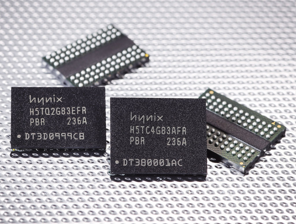
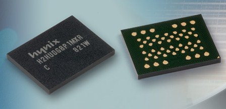
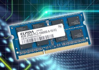
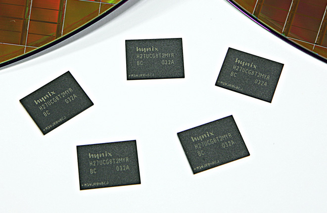
SK Hynix Introduces DDR3L-Reduced Standby for Mobile Solutions
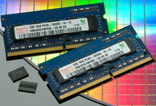
SK Hynix announced that it has introduced DDR3L-RS (Reduced Standby) DRAM for mobile solutions using its 20nm class technology. This product significantly reduces the standby power consumption.
By using cutting-edge 20nm class technology and efficiently managing standby current, this DDR3L-RS product reduces 70% of standby power compared to existing DDR3L DRAM while it maintains DDR3L performance. DDR3L DRAM which has recently gone mainstream works at 1.35V, while DDR3 DRAM does at 1.5V.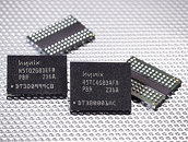
By using cutting-edge 20nm class technology and efficiently managing standby current, this DDR3L-RS product reduces 70% of standby power compared to existing DDR3L DRAM while it maintains DDR3L performance. DDR3L DRAM which has recently gone mainstream works at 1.35V, while DDR3 DRAM does at 1.5V.