News Posts matching #Interconnect

Return to Keyword Browsing

The SEA Projects Prepare Europe for Exascale Supercomputing

The HPC research projects DEEP-SEA, IO-SEA and RED-SEA are wrapping up this month after a three-year project term. The three projects worked together to develop key technologies for European Exascale supercomputers, based on the Modular Supercomputing Architecture (MSA), a blueprint architecture for highly efficient and scalable heterogeneous Exascale HPC systems. To achieve this, the three projects collaborated on system software and programming environments, data management and storage, as well as interconnects adapted to this architecture. The results of their joint work will be presented at a co-design workshop and poster session at the EuroHPC Summit (Antwerp, 18-21 March, www.eurohpcsummit.eu).

Huawei Launches OptiXtrans DC908 Pro, a Next-gen DCI Platform for the AI Era

At MWC Barcelona 2024, Huawei launched the Huawei OptiXtrans DC908 Pro, a new platform for Data Center Interconnect (DCI) designed for the intelligent era. This innovative platform ensures the efficient, secure, and stable transmission of data between data centers (DCs), setting a new standard for DCI networks. As AI continues to proliferate across various service scenarios, the demand for foundation models has intensified, leading to an explosion in data volume. DCs are now operating at the petabyte level, and DCI networks have evolved from single-wavelength 100 Gbit/s to single-wavelength Tbit/s.

In response to the challenges posed by massive data transmission in the intelligent era, Huawei introduces the next-generation DCI platform, the Huawei OptiXtrans DC908 Pro. Compared to its predecessor, the DC908 Pro offers higher bandwidth, reliability, and intelligence.

Ayar Labs Showcases 4 Tbps Optically-enabled Intel FPGA at Supercomputing 2023

Ayar Labs, a leader in silicon photonics for chip-to-chip connectivity, will showcase its in-package optical I/O solution integrated with Intel's industry-leading Agilex Field-Programmable Gate Array (FPGA) technology. In demonstrating 5x current industry bandwidth at 5x lower power and 20x lower latency, the optical FPGA - packaged in a common PCIe card form factor - has the potential to transform the high performance computing (HPC) landscape for data-intensive workloads such as generative artificial intelligence (AI), machine learning, and support novel new disaggregated compute and memory architectures and more.

"We're on the cusp of a new era in high performance computing as optical I/O becomes a 'must have' building block for meeting the exponentially growing, data-intensive demands of emerging technologies like generative AI," said Charles Wuischpard, CEO of Ayar Labs. "Showcasing the integration of Ayar Labs' silicon photonics and Intel's cutting-edge FPGA technology at Supercomputing is a concrete demonstration that optical I/O has the maturity and manufacturability needed to meet these critical demands."

Synopsys and TSMC Streamline Multi-Die System Complexity with Unified Exploration-to-Signoff Platform and Proven UCIe IP on TSMC N3E Process

Synopsys, Inc. today announced it is extending its collaboration with TSMC to advance multi-die system designs with a comprehensive solution supporting the latest 3Dblox 2.0 standard and TSMC's 3DFabric technologies. The Synopsys Multi-Die System solution includes 3DIC Compiler, a unified exploration-to-signoff platform that delivers the highest levels of design efficiency for capacity and performance. In addition, Synopsys has achieved first-pass silicon success of its Universal Chiplet Interconnect Express (UCIe) IP on TSMC's leading N3E process for seamless die-to-die connectivity.

"TSMC has been working closely with Synopsys to deliver differentiated solutions that address designers' most complex challenges from early architecture to manufacturing," said Dan Kochpatcharin, head of the Design Infrastructure Management Division at TSMC. "Our long history of collaboration with Synopsys benefits our mutual customers with optimized solutions for performance and power efficiency to help them address multi-die system design requirements for high-performance computing, data center, and automotive applications."

THX Ltd. Announces New THX Interconnect Cables to Elevate Home Theater Entertainment

THX Ltd., a world-class high-fidelity audio and video tuning, certification, and technology company, today announced it is launching THX Interconnect, designed in partnership with Pixelgen. THX Interconnect are a family of Ultra High Speed HDMI 2.1 cables capable of delivering 100% uncompressed 48 Gbps signaling to optimize the fidelity and reliability of nearly any sized or configured home theater system. THX is also relaunching its popular home theater installer THX Certified Training series. Both will be highlighted in early September in Denver, Colorado at the CEDIA Expo.

"The THX mission is to empower high-fidelity entertainment, regardless of where and how consumers want to enjoy movies, music and games," said Jason Fiber, chief executive officer, THX Ltd. "The THX Interconnect cables ensure all home theater components work in harmony at the highest resolutions, regardless of the length. We are pleased to bring home theater enthusiasts around the globe this cost-effective and incredibly reliable new solution. We also look forward to reintroducing the THX Certified Training program which has been dormant for a few years but is back due to overwhelming demand from the home theater installation industry."

Lightelligence Introduces Optical Interconnect for Composable Data Center Architectures

Lightelligence, the global leader in photonic computing and connectivity systems, today announced Photowave, the first optical communications hardware designed for PCIe and Compute Express Link (CXL) connectivity, unleashing next-generation workload efficiency.

Photowave, an Optical Networking (oNET) transceiver leveraging the significant latency and energy efficiency of photonics technology, empowers data center managers to scale resources within or across server racks. The first public demonstration of Photowave will be at Flash Memory Summit today through Thursday, August 10, in Santa Clara, Calif.

PCI-SIG Exploring an Optical Interconnect to Enable Higher PCIe Technology Performance

PCI-SIG today announced the formation of a new workgroup to deliver PCI Express (PCIe) technology over optical connections. The PCI-SIG Optical Workgroup intends to be optical technology-agnostic, supporting a wide range of optical technologies, while potentially developing technology-specific form factors.

"Optical connections will be an important advancement for PCIe architecture as they will allow for higher performance, lower power consumption, extended reach and reduced latency," said Nathan Brookwood, Research Fellow at Insight 64. "Many data-demanding markets and applications such as Cloud and Quantum Computing, Hyperscale Data Centers and High-Performance Computing will benefit from PCIe architecture leveraging optical connections."

Leaked Email Suggests AMD Instinct MI450 Accelerators to Feature XSwitch Interconnect Fabric

AMD is reported to be forming plans for its Instinct MI400 Accelerator series, according to a leaked internal email. This information was shared by a hardware tipster (HXL/@9550Pro) on Twitter, but their post has been deleted as some point today. Wccftech was quick enough to note down the details, and their report suggests that AMD is already making plans for an APU range that is set to succeed the unreleased Instinct MI300 lineup (expected later in 2023). Instinct MI400 accelerators are touted to drive next generation data center and cloud platforms.

The leaked email email contained information about three upcoming products: Weisshorn, MI450 and XSwitch. Kepler's recent tweet posits that Weisshorn is AMD's in-house moniker for Zen 6 "Morpheus" architecture-based Venice CPUs - these are alleged to form part of an upcoming EPYC lineup (slated for 2025 or 2026). Hardware experts reckon that AMD will introduce a new interconnect fabric with the MI400 series - "XSwitch" is speculated to be the company's main technological answer to NVIDIA's NVLINK.

Synopsys, TSMC and Ansys Strengthen Ecosystem Collaboration to Advance Multi-Die Systems

Accelerating the integration of heterogeneous dies to enable the next level of system scalability and functionality, Synopsys, Inc. (Nasdaq: SNPS) has strengthened its collaboration with TSMC and Ansys for multi-die system design and manufacturing. Synopsys provides the industry's most comprehensive EDA and IP solutions for multi-die systems on TSMC's advanced 7 nm, 5 nm and 3 nm process technologies with support for TSMC 3DFabric technologies and 3Dblox standard. The integration of Synopsys implementation and signoff solutions and Ansys multi-physics analysis technology on TSMC processes allows designers to tackle the biggest challenges of multi-die systems, from early exploration to architecture design with signoff power, signal and thermal integrity analysis.

"Multi-die systems provide a way forward to achieve reduced power and area and higher performance, opening the door to a new era of innovation at the system-level," said Dan Kochpatcharin, head of Design Infrastructure Management Division at TSMC. "Our long-standing collaboration with Open Innovation Platform (OIP) ecosystem partners like Synopsys and Ansys gives mutual customers a faster path to multi-die system success through a full spectrum of best-in-class EDA and IP solutions optimized for our most advanced technologies."

Winbond Joins UCIe Consortium to Support High-performance Chiplet Interface Standardisation

Winbond has joined the UCIe (Universal Chiplet Interconnect Express) Consortium, the industry Consortium dedicated to advancing UCIe technology. This open industry standard defines interconnect between chiplets within a package, enabling an open chiplet ecosystem and facilitating the development of advanced 2.5D/3D devices.

A leader in high-performance memory ICs, Winbond is an established supplier of known good die (KGD) needed to assure end-of-line yield in 2.5D/3D assembly. 2.5D/3D multichip devices are needed to realize the exponential improvements in performance, power efficiency, and miniaturization, demanded by the explosion of technologies such as 5G, Automotive, and Artificial Intelligence (AI).

Eliyan Closes $40M Series A Funding Round and Unveils Industry's Highest Performance Chiplet Interconnect Technologies

Eliyan Corporation, credited for the invention of the semiconductor industry's highest-performance and most efficient chiplet interconnect, today announced two major milestones in the commercialization of its technology for multi-die chiplet integration: the close of its Series A $40M funding round, and the successful tapeout of its technology on an industry standard 5-nanometer (nm) process.

Eliyan's NuLink PHY and NuGear technologies address the critical need for a commercially viable approach to enabling high performance and cost-effectiveness in the connection of homogeneous and heterogenous architectures on a standard, organic chip substrate. It has proven to achieve similar bandwidth, power efficiency, and latency as die-to-die implementations using advanced packaging technologies, but without the other drawbacks of specialized approaches.

AMD-Powered Frontier Supercomputer Faces Difficulties, Can't Operate a Day without Issues

When AMD announced that the company would deliver the world's fastest supercomputer, Frontier, the company also took a massive task to provide a machine capable of producing one ExaFLOP of total sustained ability to perform computing tasks. While the system is finally up and running, making a machine of that size run properly is challenging. In the world of High-Performance Computing, getting the hardware is only a portion of running the HPC center. In an interview with InsideHPC, Justin Whitt, program director for the Oak Ridge Leadership Computing Facility (OLCF), provided insight into what it is like to run the world's fastest supercomputer and what kinds of issues it is facing.

The Frontier system is powered by AMD EPYC 7A53s "Trento" 64-core 2.0 GHz CPUs and Instinct MI250X GPUs. Interconnecting everything is the HPE (Cray) Slingshot 64-port switch, which is responsible for sending data in and out of compute blades. The recent interview points out a rather interesting finding: exactly AMD Instinct MI250X GPUs and Slingshot interconnect cause hardware troubles for the Frontier. "It's mostly issues of scale coupled with the breadth of applications, so the issues we're encountering mostly relate to running very, very large jobs using the entire system … and getting all the hardware to work in concert to do that," says Justin Whitt. In addition to the limits of scale "The issues span lots of different categories, the GPUs are just one. A lot of challenges are focused around those, but that's not the majority of the challenges that we're seeing," he said. "It's a pretty good spread among common culprits of parts failures that have been a big part of it. I don't think that at this point that we have a lot of concern over the AMD products. We're dealing with a lot of the early-life kind of things we've seen with other machines that we've deployed, so it's nothing too out of the ordinary."

AMD's CEO Lisa Su Planning Trip to Taiwan, Said to be Visiting TSMC to Secure Future Wafer Allocation

Based on a report by Tom's Hardware, AMD's CEO Lisa Su is planning a trip to Taiwan in the next couple of months. It is said that she is planning to meet with multiple partners in Taiwan, such as ASUS, Acer and maybe more importantly, ASMedia, which will be the sole maker of chipsets for AMD, once the X570 chipset is discontinued. AMD is apparently also seeing various less well known partners that deliver parts for its CPUs, such as Nan Ya PCB, Unimicron Technologies and Kinsus Interconnects.

However, it appears that the main reason for Lisa Su herself to visit Taiwan will be to meet with TSMC, to discuss future collaboration with CC Wei, TSMC's chief executive. This is so AMD can secure enough wafer allocation on future nodes, such as its 3 nm and 2 nm class nodes. The move to these nodes is obviously not happening in the near future for AMD, but considering that TSMC is currently the leading foundry and is operating at capacity, it makes sense to get in early, as the competition is stiff when it comes to getting wafer allocation on cutting edge nodes. It's unclear which exact 3 nm class node AMD will be aiming for, but it might be the N3P node, which is said to kick off production sometime next year. Lisa Su is also said to have meetings with TSMC, SPIL and Ase Technology when it comes to advanced packaging for AMD's products. This includes technologies such as chip-on-wafer-on-substrate (CoWoS) and fan-out embedded bridge (FO-EB), with AMD already being expected to use some of these technologies in its upcoming Navi 3x GPUs.

BittWare Announces PCIe 5.0/CXL FPGA Accelerators Featuring Intel Agilex M-Series and I-Series to Drive Memory and Interconnectivity Improvements

BittWare, a Molex company, a leading supplier of enterprise-class accelerators for edge and cloud-computing applications, today introduced new card and server-level solutions featuring Intel Agilex FPGAs. The new BittWare IA-860m helps customers alleviate memory-bound application workloads by leveraging up to 32 GB of HBM2E in-package memory and 16-lanes of PCIe 5.0 (with CXL upgrade option). BittWare also added new Intel Agilex I-Series FPGA-based products with the introduction of the IA-440i and IA-640i accelerators, which support high-performance interfaces, including 400G Ethernet and PCIe 5.0 (CXL option). These newest models complement BittWare's existing lineup of Intel Agilex F-Series products to comprise one of the broadest portfolios of Intel Agilex FPGA-based offerings on the market. This announcement reinforces BittWare's commitment to addressing ever-increasing demands of high-performance compute, storage, network and sensor processing applications.

"BittWare is excited to apply Intel's advanced technology to solve increasingly difficult application problems, quickly and at low risk," said Craig Petrie, vice president, Sales and Marketing of BittWare. "Our longstanding collaboration with Intel, expertise with the latest development tools, including OneAPI, as well as alignment with Molex's global supply chain and manufacturing capabilities enable BittWare to reduce development time by 12-to-18 months while ensuring smooth transitions from proof-of-concept to volume product deployment."

Avicena Raises $25 Million in Series A to Fund Development of High Capacity microLED-based Optical Interconnects

-AvicenaTech Corp., the leader in microLED-based chip-to-chip interconnects, today announced that the company has secured $25M in Series A funding from Samsung Catalyst Fund, Cerberus Capital Management, Clear Ventures, and Micron Ventures to drive the development of products based on Avicena's breakthrough photonic I/O solution. "We believe that Avicena technology can be transformational in unlocking compute-to-memory chip-to-chip high-speed interconnects. Such technology can be central to supporting future disaggregated architectures and distributed high-performance computing (HPC) systems," said Marco Chisari, EVP of Samsung Electronics and Head of the Samsung Semiconductor Innovation Center.

"We are excited to participate in this round at Avicena," said Amir Salek, Senior Managing Director at Cerberus Capital Management and former Head of silicon for Google Infrastructure and Cloud. "Avicena has a highly differentiated technology addressing one of the main challenges in modern computer architecture. The technology offered by Avicena meets the needs for scaling future HPC and cloud compute networks and covers applications in conventional datacenter and 5G cellular networking."

Ayar Labs Partners with NVIDIA to Deliver Light-Based Interconnect for AI Architectures

Ayar Labs, the leader in chip-to-chip optical connectivity, is developing with NVIDIA groundbreaking artificial intelligence (AI) infrastructure based on optical I/O technology to meet future demands of AI and high performance computing (HPC) workloads. The collaboration will focus on integrating Ayar Labs' technology to develop scale-out architectures enabled by high-bandwidth, low-latency and ultra-low-power optical-based interconnects for future NVIDIA products. Together, the companies plan to accelerate the development and adoption of optical I/O technology to support the explosive growth of AI and machine learning (ML) applications and data volumes.

Optical I/O uniquely changes the performance and power trajectories of system designs by enabling compute, memory and networking ASICs to communicate with dramatically increased bandwidth, at lower latency, over longer distances and at a fraction of the power of existing electrical I/O solutions. The technology is also foundational to enabling emerging heterogeneous compute systems, disaggregated/pooled designs, and unified memory architectures that are critical to accelerating future data center innovation.

Rambus to Acquire Hardent, Accelerating Roadmap for Next-Generation Data Center Solutions

-Rambus Inc., a provider of industry-leading chips and silicon IP making data faster and safer, today announced it has signed an agreement to acquire Hardent, Inc. ("Hardent"), a leading electronic design company. This acquisition augments the world-class team of engineers at Rambus and accelerates the development of CXL processing solutions for next-generation data centers. With 20 years of semiconductor experience, Hardent's world-class silicon design, verification, compression, and Error Correction Code (ECC) expertise provides key resources for the Rambus CXL Memory Interconnect Initiative.

"Driven by the demands of advanced workloads like AI/ML and the move to disaggregated data center architectures, industry momentum for CXL-based solutions continues to grow," said Luc Seraphin, president and CEO of Rambus. "The addition of the highly-skilled Hardent design team brings key resources that will accelerate our roadmap and expand our reach to address customer needs for next-generation data center solutions." "The Rambus culture and track record of technology leadership is an ideal fit for Hardent," said Simon Robin, president and founder of Hardent. "The team is looking forward to joining Rambus and is excited to be part of a global company advancing the future of data center solutions." In addition, Hardent brings complementary IP and services to the Rambus silicon IP portfolio, expanding the customer base and design wins in automotive and consumer electronic applications. The transaction is expected to close in the second calendar quarter of 2022 and will not materially impact results.

NVIDIA Opens NVLink for Custom Silicon Integration

Enabling a new generation of system-level integration in data centers, NVIDIA today announced NVIDIA NVLink -C2C, an ultra-fast chip-to-chip and die-to-die interconnect that will allow custom dies to coherently interconnect to the company's GPUs, CPUs, DPUs, NICs and SOCs. With advanced packaging, NVIDIA NVLink-C2C interconnect would deliver up to 25x more energy efficiency and be 90x more area-efficient than PCIe Gen 5 on NVIDIA chips and enable coherent interconnect bandwidth of 900 gigabytes per second or higher.

"Chiplets and heterogeneous computing are necessary to counter the slowing of Moore's law," said Ian Buck, vice president of Hyperscale Computing at NVIDIA. "We've used our world-class expertise in high-speed interconnects to build uniform, open technology that will help our GPUs, DPUs, NICs, CPUs and SoCs create a new class of integrated products built via chiplets."

Intel, AMD, Arm, and Others, Collaborate on UCIe (Universal Chiplet Interconnect Express)

Intel, along with Advanced Semiconductor Engineering Inc. (ASE), AMD, Arm, Google Cloud, Meta, Microsoft Corp., Qualcomm Inc., Samsung and Taiwan Semiconductor Manufacturing Co., have announced the establishment of an industry consortium to promote an open die-to-die interconnect standard called Universal Chiplet Interconnect Express (UCIe). Building on its work on the open Advanced Interface Bus (AIB), Intel developed the UCIe standard and donated it to the group of founding members as an open specification that defines the interconnect between chiplets within a package, enabling an open chiplet ecosystem and ubiquitous interconnect at the package level.

"Integrating multiple chiplets in a package to deliver product innovation across market segments is the future of the semiconductor industry and a pillar of Intel's IDM 2.0 strategy," said Sandra Rivera, executive vice president and general manager of the Datacenter and Artificial Intelligence Group at Intel. "Critical to this future is an open chiplet ecosystem with key industry partners working together under the UCIe Consortium toward a common goal of transforming the way the industry delivers new products and continues to deliver on the promise of Moore's Law."

CXL Consortium & Gen-Z Consortium Sign Letter of Intent to Advance Interconnect Technology

High performance computing continues to evolve—meeting the ever-increasing demand for high efficiency, low-latency, rapid and seamless processing. The Gen-Z Consortium was founded in 2016 to create a next-generation fabric capable of bridging existing solutions while enabling new, unbounded innovation in an open, non-proprietary standards body.

In 2019, the CXL Consortium launched to deliver Compute Express Link (CXL ), an industry-supported cache-coherent interconnect designed for processors, memory expansion, and accelerators. The CXL Consortium and the Gen-Z Consortium established a joint memorandum of understanding (MOU) providing an opportunity for collaboration to define bridging between the protocols. This took the form of a joint working group that encouraged creativity and innovation between the two organizations toward the betterment of the industry as a whole.

Samsung Announces Availability of Its Leading-Edge 2.5D Integration H-Cube Solution

Samsung Electronics, a world leader in advanced semiconductor technology, today announced that it has developed Hybrid-Substrate Cube (H-Cube) technology, its latest 2.5D packaging solution specialized for semiconductors for HPC, AI, data center, and network products that require high-performance and large-area packaging technology.

"H-Cube solution, which is jointly developed with Samsung Electro-mechanics (SEMCO) and Amkor Technology, is suited to high-performance semiconductors that need to integrate a large number of silicon dies," said Moonsoo Kang, senior vice president and Head of Foundry Market Strategy Team at Samsung Electronics. "By expanding and enriching the foundry ecosystem, we will provide various package solutions to find a breakthrough in the challenges our customers are facing."

"Zen 3" Chiplet Uses a Ringbus, AMD May Need to Transition to Mesh for Core-Count Growth

AMD's "Zen 3" CCD, or compute complex die, the physical building-block of both its client- and enterprise processors, possibly has a core count limitation owing to the way the various on-die bandwidth-heavy components are interconnected, says an AnandTech report. This cites what is possibly the first insights AMD provided on the CCD's switching fabric, which confirms the presence of a Ring Bus topology. More specifically, the "Zen 3" CCD uses a bi-directional Ring Bus to connect the eight CPU cores with the 32 MB of shared L3 cache, and other key components of the CCD, such as the IFOP interface that lets the CCD talk to the I/O die (IOD).

Imagine a literal bus driving around a city block, picking up and dropping off people between four buildings. The "bus" here resembles a strobe, the buildings resemble components (cores, uncore, etc.,) while the the bus-stops are ring-stops. Each component has its ring-stops. To disable components (eg: in product-stack segmentation), SKU designers simply disable ring-stops, making the component inaccessible. A bi-directional Ring Bus would see two "vehicles" driving in opposite directions around the city block. The Ring Bus topology comes with limitations of scale, mainly resulting from the latency added from too many ring-stops. This is precisely why coaxial ring-topology faded out in networking.

Intel and QuTech Demonstrate Advances in Solving Quantum Interconnect Bottlenecks

Today, Intel and QuTech—a collaboration between Delft University of Technology and the Netherlands Organisation for Applied Scientific Research - published key findings in quantum research to address the "interconnect bottleneck" that exists between quantum chips that sit in cryogenic dilution refrigerators and the complex room-temperature electronics that control the qubits. The innovations were covered in Nature, the industry-leading science journal of peer-reviewed research, and mark an important milestone in addressing one of the biggest challenges to quantum scalability with Intel's cryogenic controller chip Horse Ridge.

"Our research results, driven in partnership with QuTech, quantitatively prove that our cryogenic controller, Horse Ridge, can achieve the same high-fidelity results as room-temperature electronics while controlling multiple silicon qubits. We also successfully demonstrated frequency multiplexing on two qubits using a single cable, which clears the way for simplifying the "wiring challenge" in quantum computing. Together, these innovations pave the way for fully integrating quantum control chips with the quantum processor in the future, lifting a major roadblock in quantum scaling," said Stefano Pellerano, principal engineer at Intel Labs.

Samsung Unveils Industry-First Memory Module Incorporating New CXL Interconnect

Samsung Electronics Co., Ltd., the world leader in advanced memory technology, today unveiled the industry's first memory module supporting the new Compute Express Link (CXL) interconnect standard. Integrated with Samsung's Double Data Rate 5 (DDR5) technology, this CXL-based module will enable server systems to significantly scale memory capacity and bandwidth, accelerating artificial intelligence (AI) and high-performance computing (HPC) workloads in data centers.

The rise of AI and big data has been fueling the trend toward heterogeneous computing, where multiple processors work in parallel to process massive volumes of data. CXL—an open, industry-supported interconnect based on the PCI Express (PCIe) 5.0 interface—enables high-speed, low latency communication between the host processor and devices such as accelerators, memory buffers and smart I/O devices, while expanding memory capacity and bandwidth well beyond what is possible today. Samsung has been collaborating with several data center, server and chipset manufacturers to develop next-generation interface technology since the CXL consortium was formed in 2019.

Lian Li Launches New Fan Interlocking System with the UNI FAN SL120

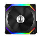
LIAN LI Industrial Co. Ltd., a leading manufacturer of aluminium chassis and PC accessories, announces the UNI FAN SL120, an innovative approach to reducing cables by interlocking and daisy-chaining the fans. Designed as 120 mm high static pressure PWM fans with addressable RGB LEDs, the UNI FAN SL120 has a newly patented quick-connect daisy-chaining style system that simplifies cable management and mounting efforts. With up to 16 fans (4 sets of 4) under one fan controller, users can easily create an adapted profile to match their fan speed and synchronized lighting effect needs via the highly intuitive L-Connect software. Available in black or white, the UNI FAN SL120 offers a new premium look with lighting effects that do not compromise on performance.

Focused on giving users more control over fan functionality, the clean and intuitive interface of the L-Connect software provides instant speed and RGB light management for individual fans or simultaneous control over all 4 clusters of fans. With 5 fan speed profiles, 14 lighting effects, and control over each effect's color, brightness, direction, and speed, L-Connect allows full customization of the look and feel of the system. Alternatively, users can choose to sync with the motherboard software via the simple toggle of a switch.
Return to Keyword Browsing
May 1st, 2024 02:03 EDT change timezone

New Forum Posts

Popular Reviews

Controversial News Posts