News Posts matching #MCM

Return to Keyword Browsing

Intel Xe Graphics to Feature MCM-like Configurations, up to 512 EU on 500 W TDP

A reportedly leaked Intel slide via DigitalTrends has given us a load of information on Intel's upcoming take on the high performance graphics accelerators market - whether in its server or consumer iterations. Intel's Xe has already been cause for much discussion in a market that has only really seen two real competitors for ages now - the coming of a third player with muscles and brawl such as Intel against the already-established players NVIDIA and AMD would surely spark competition in the segment - and competition is the lifeblood of advancement, as we've recently seen with AMD's Ryzen CPU line.

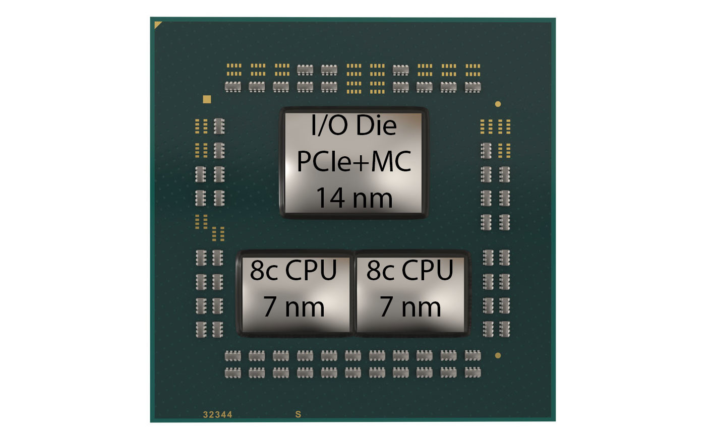
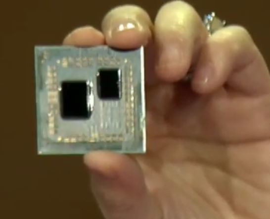
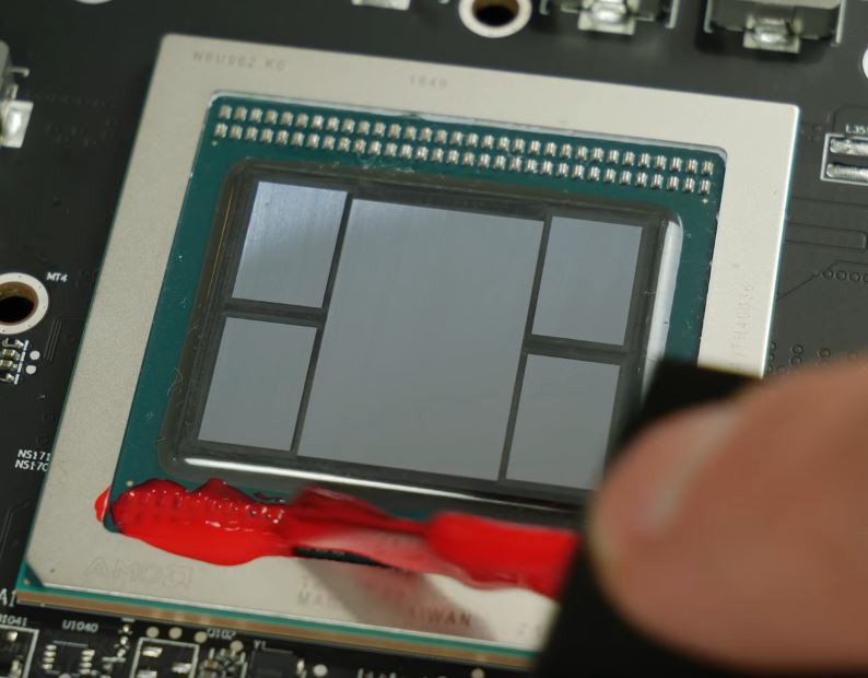
The leaked slide reveals that Intel will be looking to employ a Multi-Chip-Module (MCM) approach to its high performance "Arctic Sound" graphics architecture. The GPUs will be available in up to 4-tile configuration (the name Intel is giving each module), which will then be joined via Foveros 3D stacking (first employed in Intel Lakefield. This leaked slide shows Intel's approach starting with a 1-tile GPU (with only 96 of its 128 total EUs active) for the entry level market (at 75 W TDP) a-la DG1 SDV (Software Development Vehicle).

NVIDIA Files for "Hopper" and "Aerial" Trademarks

In a confirmation that a future NVIDIA graphics architecture will be codenamed "Hopper," the company has trademarked the term with the US-PTO. The trademark application was filed as recently as December 4, and closely follows that of "Aerial," another trademark, which is an SDK for a GPU-accelerated 5G vRANs (virtual radio-access networks). Named after eminent computing scientist Grace Hopper, the new graphics architecture by NVIDIA reportedly sees one of the first GPU die MCMs (package with multiple GPU dies). It reportedly succeeds "Ampere," NVIDIA's next graphics architecture.

NVIDIA "Ampere" Successor Reportedly Codenamed "Hopper"

NVIDIA has reportedly codenamed a future GPU architecture "Hopper," in honor of Grace Hopper, an eminent computer scientist who invented one of the first linkers, and programmed the Harvard Mark I computer that aided the American war efforts in World War II. This came to light as Twitter user "@kopite7kimi," who's had a fairly high hit-rate with NVIDIA info tweeted not just the codename, but also a key NVIDIA product design change. The tweets were later deleted, but not before 3DCenter.org reported on them. To begin with, "Hopper" is reportedly succeeding the upcoming "Ampere" architecture slated for the first half of 2020.

"Hopper" is also rumored to introduce MCM (multi-chip module) GPU packages, which are packages with multiple GPU dies. Currently, GPU MCMs are packages that have one GPU die surrounded by memory dies or stacks. This combination of GPU dies could make up "giant cores," at least in the higher end of the performance spectrum. NVIDIA reserves MCMs for only its most expensive Tesla family of compute accelerators, or Quadro professional graphics cards, and seldom offers client-segment GeForce products.

AMD Readies Three HEDT Chipsets: TRX40, TRX80, and WRX80

AMD is preparing to surprise Intel with its 3rd generation Ryzen Threadripper processors derived from the "Rome" MCM (codenamed "Castle Peak" for the client-platform), that features up to 64 CPU cores, a monolithic 8-channel DDR4 memory interface, and 128 PCIe gen 4.0 lanes. For the HEDT platform, AMD could reconfigure the I/O controller die for two distinct sub-platforms within HEDT - one targeting gamers/enthusiasts, and another targeting the demographic that buys Xeon W processors, including the W-3175X. The gamer/enthusiast-targeted processor line could feature a monolithic 4-channel DDR4 memory interface, and 64 PCI-Express gen 4.0 lanes from the processor socket, and additional lanes from the chipset; while the workstation-targeted processor line could essentially be EPYCs, with a wider memory bus width and more platform PCIe lanes; while retaining drop-in backwards-compatibility with AMD X399 (at the cost of physically narrower memory and PCIe I/O).

To support this diverse line of processors, AMD is coming up with not one, but three new chipsets: TRX40, TRX80, and WRX80. The TRX40 could have a lighter I/O feature-set (similar to the X570), and probably 4-channel memory on the motherboards. The TRX80 and WRX80 could leverage the full I/O of the "Rome" MCM, with 8-channel memory and more than 64 PCIe lanes. We're not sure what differentiates the TRX80 and WRX80, but we believe motherboards based on the latter will resemble proper workstation boards in form-factors such as SSI, and be made by enterprise motherboard manufacturers such as TYAN. The chipsets made their way to the USB-IF for certification, and were sniffed out by momomo_us. ASUS is ready with its first motherboards based on the TRX40, the Prime TRX40-Pro, and the ROG Strix TRX40-E Gaming.

AMD CEO Lisa Su: "CrossFire Isn't a Significant Focus"

AMD CEO Lisa Su at the Hot Chips conference answered some questions from the attending press. One of these regarded AMD's stance on CrossFire and whether or not it remains a focus for the company. Once the poster child for a scalable consumer graphics future, with AMD even going as far as enabling mixed-GPU support (with debatable merits). Lisa Su came out and said what we all have been seeing happening in the background: "To be honest, the software is going faster than the hardware, I would say that CrossFire isn't a significant focus".

There isn't anything really new here; we've all seen the consumer GPU trends as of late, with CrossFire barely being deserving of mention (and the NVIDIA camp does the same for their SLI technology, which has been cut from all but the higher-tier graphics cards). Support seems to be enabled as more of an afterthought than a "focus", and that's just the way things are. It seems that the old, old practice of buying a lower-tier GPU at launch and then buying an additional graphics processor further down the line to leapfrog performance of higher-performance, single GPU solutions is going the way of the proverbial dodo - at least until an MCM (Multi-Chip-Module) approach sees the light of day, paired with a hardware syncing solution that does away with the software side of things. A true, integrated, software-blind multi-GPU solution comprised of two or more smaller dies than a single monolithic solution seems to be the way to go. We'll see.

AMD Designing Zen 4 for 2021, Zen 3 Completes Design Phase, out in 2020

AMD in its 2nd generation EPYC processor launch event announced that it has completed the design phase of its next-generation "Zen 3" CPU microarchitecture, and is currently working on its successor, the "Zen 4." AMD debuted its "Zen 2" microarchitecture with the client-segment 3rd generation Ryzen desktop processor family, it made its enterprise debut with the 2nd generation EPYC. This is the first x86 CPU microarchitecture designed for the 7 nanometer silicon fabrication process, and is being built on a 7 nm DUV (deep ultraviolet) node at TSMC. It brings about double-digit percentage IPC improvements over "Zen+."

The "Zen 3" microarchitecture is designed for the next big process technology change within 7 nm, EUV (extreme ultraviolet), which allows significant increases in transistor densities, and could facilitate big improvements in energy-efficiency that could be leveraged to increase clock-speeds and performance. It could also feature new ISA instruction-sets. With "Zen 3" passing design phase, AMD will work on prototyping and testing it. The first "Zen 3" products could debut in 2020. "Zen 4" is being designed for a different era.

AMD Retires the Radeon VII Less Than Five Months Into Launch

AMD has reportedly discontinued production of its flagship Radeon VII graphics card. According to a Cowcotland report, AMD no longer finds it viable to produce and sell the Radeon VII at prices competitive to NVIDIA's RTX 2080, especially when its latest Radeon RX 5700 XT performs within 5-12 percent of the Radeon VII at less than half its price. AMD probably expects custom-design RX 5700 XT cards to narrow the gap even more. The RX 5700 XT has a much lesser BOM (bill of materials) cost compared to the Radeon VII, due to the simplicity of its ASIC, a conventional GDDR6 memory setup, and far lighter electrical requirements.

In stark contrast to the RX 5700 XT, the Radeon VII is based on a complex MCM (multi-chip module) that has not just a 7 nm GPU die, but also four 32 Gbit HBM2 stacks, and a silicon interposer. It also has much steeper VRM requirements. Making matters worse is the now-obsolete "Vega" architecture it's based on, which loses big time against "Navi" at performance/Watt. The future of AMD's high-end VGA lineup is uncertain. Looking at the way "Navi" comes close to performance/Watt parity with NVIDIA on the RX 5700, AMD may be tempted to design a larger GPU die based on "Navi," with a conventional GDDR6-based memory sub-system, to take another swing at NVIDIA's high-end.

Bitspower Unveils the Touchaqua CPU Block Summit MS For AM4 Processors

Bitspower today unveiled the Touchaqua series Summit MS for AMD socket AM4. The block is designed for full coverage of the AMD socket AM4 processor IHS, and can uniformly cool even the latest "Matisse" MCMs since its micro-fin lattice is spread across a wider area than most other socket AM4 blocks. The primary material is copper, with a central portion that has a mirror-finish; while the top is made of acrylic with an embedded addressable-RGB strip that takes in 3-pin aRGB input. The block measures 111 mm x 73 mm x 20.3 mm (LxWxH), and takes in standard G 1/4" fittings. The block is now available for pre-order from Bitspower website.

AMD Ryzen 3000 "Matisse" I/O Controller Die 12nm, Not 14nm

AMD Ryzen 3000 "Matisse" processors are multi-chip modules of two kinds of dies - one or two 7 nm 8-core "Zen 2" CPU chiplets, and an I/O controller die that packs the processor's dual-channel DDR4 memory controller, PCI-Express gen 4.0 root-complex, and an integrated southbridge that puts out some SoC I/O, such as two SATA 6 Gbps ports, four USB 3.1 Gen 2 ports, LPCIO (ISA), and SPI (for the UEFI BIOS ROM chip). It was earlier reported that while the Zen 2 CPU core chiplets are built on 7 nm process, the I/O controller is 14 nm. We have confirmation now that the I/O controller die is built on the more advanced 12 nm process, likely GlobalFoundries 12LP. This is the same process on which AMD builds its "Pinnacle Ridge" and "Polaris 30" chips. The 7 nm "Zen 2" CPU chiplets are made at TSMC.

AMD also provided a fascinating technical insight to the making of the "Matisse" MCM, particularly getting three highly complex dies under the IHS of a mainstream-desktop processor package, and perfectly aligning the three for pin-compatibility with older generations of Ryzen AM4 processors that use monolithic dies, such as "Pinnacle Ridge" and "Raven Ridge." AMD innovated new copper-pillar 50µ bumps for the 8-core CPU chiplets, while leaving the I/O controller die with normal 75µ solder bumps. Unlike with its GPUs that need high-density wiring between the GPU die and HBM stacks, AMD could make do without a silicon interposer or TSVs (through-silicon-vias) to connect the three dies on "Matisse." The fiberglass substrate is now "fattened" up to 12 layers, to facilitate the inter-die wiring, as well as making sure every connection reaches the correct pin on the µPGA.

AMD Readies Ryzen 9 3950X 16-core Processor to Awestrike Crowds at E3

When AMD launched its Ryzen 9 3900X 12-core/24-thread processor at its Computex 2019 keynote, our readers commented on the notable absence of a 16-core SKU, given that a "Matisse" multi-chip module with two 8-core "Zen 2" chiplets adds up to that core-count. Some readers noted this could be a case of AMD holding back its top performing part in the absence of competition in the segment from Intel. It turns out, the company was saving this part up for an E3 2019 unveiling.

The Ryzen 9 3950X maxes out "Matisse" MCM with 16 cores, 32 threads via SMT, a staggering 64 MB of L3 cache (72 MB including the 8 MB of total L2 cache), and a stunning 105-Watt TDP figure that's unchanged from the company's TDP for the 3900X. The Ryzen 9 3950X is clocked at 3.50 GHz, with a maximum boost frequency of 4.70 GHz. The company is yet to reveal its price, but given that the $499 price-tag has already been taken by the 3900X, one could expect an even higher price. It remains to be seen if the 3950X will launch alongside the rest of the series on 7/7.

AMD Announces the Radeon Pro Vega II and Pro Vega II Duo Graphics Cards

AMD today announced the Radeon Pro Vega II and Pro Vega II Duo graphics cards, making their debut with the new Apple Mac Pro workstation. Based on an enhanced 32 GB variant of the 7 nm "Vega 20" MCM, the Radeon Pro Vega II maxes out its GPU silicon, with 4,096 stream processors, 1.70 GHz peak engine clock, 32 GB of 4096-bit HBM2 memory, and 1 TB/s of memory bandwidth. The card features both PCI-Express 3.0 x16 and InfinityFabric interfaces. As its name suggests, the Pro Vega II is designed for professional workloads, and comes with certifications for nearly all professional content creation applications.

The Radeon Pro Vega II Duo is the first dual-GPU graphics card from AMD in ages. Purpose built for the Mac Pro (and available on the Apple workstation only), this card puts two fully unlocked "Vega 20" MCMs with 32 GB HBM2 memory each on a single PCB. The card uses a bridge chip to connect the two GPUs to the system bus, but in addition, has an 84.5 GB/s InfinityFabric link running between the two GPUs, for rapid memory access, GPU and memory virtualization, and interoperability between the two GPUs, bypassing the host system bus. In addition to certifications for every conceivable content creation suite for the MacOS platform, AMD dropped in heavy optimization for the Metal 3D graphics API. For now the two graphics cards are only available as options for the Apple Mac Pro. The single-GPU Pro Vega II may see standalone product availability later this year, but the Pro Vega II Duo will remain a Mac Pro-exclusive.

TechPowerUp Releases GPU-Z v2.21.0

TechPowerUp GPU-Z is a handy graphics subsystem information, diagnostic, and monitoring utility no enthusiast can leave home without, and today we bring you its latest version. The new TechPowerUp GPU-Z v2.21.0 adds support for NVIDIA Quadro P500. More importantly, it fixes sensor data readouts being broken for the Radeon VII with Radeon Software 19.5.1 (or later) installed. A broken GPU load sensor for AMD "Raven Ridge" APUs has also been fixed. Lastly, OpenCL support detection has been added for Radeon VII and other graphics cards based on the "Vega 20" MCM. Grab it from the link below.
DOWNLOAD: TechPowerUp GPU-Z

The change-log follows.

Intel Switches Gears to 7nm Post 10nm, First Node Live in 2021

Intel's semiconductor manufacturing business has had a terrible past 5 years as it struggled to execute its 10 nanometer roadmap forcing the company's processor designers to re-hash the "Skylake" microarchitecture for 5 generations of Core processors, including the upcoming "Comet Lake." Its truly next-generation microarchitecture, codenamed "Ice Lake," which features a new CPU core design called "Sunny Cove," comes out toward the end of 2019, with desktop rollouts expected 2020. It turns out that the 10 nm process it's designed for, will have a rather short reign at Intel's fabs. Speaking at an investor's summit on Wednesday, Intel put out its silicon fabrication roadmap that sees an accelerated roll-out of Intel's own 7 nm process.

When it goes live and fit for mass production some time in 2021, Intel's 7 nm process will be a staggering 3 years behind TSMC, which fired up its 7 nm node in 2018. AMD is already mass-producing CPUs and GPUs on this node. Unlike TSMC, Intel will implement EUV (extreme ultraviolet) lithography straightaway. TSMC began 7 nm with DUV (deep ultraviolet) in 2018, and its EUV node went live in March. Samsung's 7 nm EUV node went up last October. Intel's roadmap doesn't show a leap from its current 10 nm node to 7 nm EUV, though. Intel will refine the 10 nm node to squeeze out energy-efficiency, with a refreshed 10 nm+ node that goes live some time in 2020.

AMD Ryzen 3 3200G Pictured and De-lidded

AMD Ryzen 3 3200G is an upcoming processor featuring integrated graphics, forming the tail-end of the company's 3rd generation Ryzen desktop processor family. A Chinese PC enthusiast with access to an early sample pictured and de-lidded the processor. We know from older posts that while the "Matisse" MCM will form the bulk of AMD's 3rd gen Ryzen lineup, with core counts ranging all the way from 6 to 12, and possibly 16 later, the APU lineup is rumored to be based on older "Zen+" architecture.

The Ryzen 3 3200G and possibly the Ryzen 5 3400G, will be based on a derivative of the "Raven Ridge" silicon built on the 12 nm process at GlobalFoundries, and comes with a handful innovations AMD introduced with "Pinnacle Ridge," such as an improved Precision Boost algorithm and faster on-die caches. The 12 nm shrink also allows AMD to dial up CPU and iGPU engine clock speeds, and improve DDR4 memory support to work with higher DRAM clock speeds. AMD has used thermal paste as the sub-IHS interface material instead of solder for its "Raven Ridge" chips, and the story repeats with the 3200G.

Intel Unleashes 56-core Xeon "Cascade Lake" Processor to Preempt 64-core EPYC

Intel late Tuesday made a boat-load of enterprise-relevant product announcements, including the all important update to its Xeon Scalable enterprise processor product-stack, with the addition of the new 56-core Xeon Scalable "Cascade Lake" processor. This chip is believed to be Intel's first response to the upcoming AMD 7 nm EPYC "Rome" processor with 64 cores and a monolithic memory interface. The 56-core "Cascade Lake" is a multi-chip module (MCM) of two 28-core dies, each with a 6-channel DDR4 memory interface, totaling 12-channel for the package. Each of the two 28-core dies are built on the existing 14 nm++ silicon fabrication process, and the IPC of each of the 56 cores are largely unchanged since "Skylake." Intel however, has added several HPC and AI-relevant instruction-sets.

To begin with, Intel introduced DL Boost, which could be a fixed-function hardware matrix multiplier that accelerates building and training of AI deep-learning neural networks. Next up, are hardware mitigation against several speculative execution CPU security vulnerabilities that haunted the computing world since early-2018, including certain variants of "Spectre" and "Meltdown." A hardware fix presents lesser performance impact compared to a software fix in the form of a firmware patch. Intel has added support for Optane Persistent Memory, which is the company's grand vision for what succeeds volatile primary memory such as DRAM. Currently slower than DRAM but faster than SSDs, Optane Persistent Memory is non-volatile, and its contents can be made to survive power-outages. This allows sysadmins to power-down entire servers to scale down with workloads, without worrying about long wait times to restore uptime when waking up those servers. Among the CPU instruction-sets added include AVX-512 and AES-NI.

AMD to Simultaneously Launch 3rd Gen Ryzen and Unveil Radeon "Navi" This June

TAITRA, the governing body behind the annual Computex trade-show held in Taipei each June, announced that AMD CEO Dr. Lisa Su will host a keynote address which promises to be as exciting as her CES keynote. It is revealed that Dr. Su will simultaneously launch or unveil at least four product lines. High up the agenda is AMD's highly anticipated 3rd generation Ryzen desktop processors in the socket AM4 package, based on "Zen 2" microarchitecture, and a multi-chip module (MCM) codenamed "Matisse." This launch could be followed up by a major announcement related to the company's 2nd generation EPYC enterprise processors based on the "Rome" MCM.

PC enthusiasts are in for a second major announcement, this time from RTG, with a technical reveal or unveiling of Radeon "Navi," the company's first GPU designed from the ground up for the 7 nm silicon fabrication process. It remains to be seen which market-segment AMD targets with the first "Navi" products, and the question on everyone's minds, whether AMD added DXR acceleration, could be answered. Lastly, the company could announce more variants of its Radeon Instinct DNN accelerators.

AMD Ryzen 3000 "Zen 2" BIOS Analysis Reveals New Options for Overclocking & Tweaking

AMD will launch its 3rd generation Ryzen 3000 Socket AM4 desktop processors in 2019, with a product unveiling expected mid-year, likely on the sidelines of Computex 2019. AMD is keeping its promise of making these chips backwards compatible with existing Socket AM4 motherboards. To that effect, motherboard vendors such as ASUS and MSI began rolling out BIOS updates with AGESA-Combo 0.0.7.x microcode, which adds initial support for the platform to run and validate engineering samples of the upcoming "Zen 2" chips.

At CES 2019, AMD unveiled more technical details and a prototype of a 3rd generation Ryzen socket AM4 processor. The company confirmed that it will implement a multi-chip module (MCM) design even for their mainstream-desktop processor, in which it will use one or two 7 nm "Zen 2" CPU core chiplets, which talk to a 14 nm I/O controller die over Infinity Fabric. The two biggest components of the IO die are the PCI-Express root complex, and the all-important dual-channel DDR4 memory controller. We bring you never before reported details of this memory controller.

AMD May Offer Some Insights on Upcoming Ryzen 3000 Series at GDC 2019

AMD's Ryzen 3000 series is one of the most hotly anticipated hardware launches in recent times. I'd say that the hype surrounding AMD's processor launches, unlike Intel's, has become vested with an actual enthusiasm that is likely in our nature - to see the underdog come out with innovative products that reverse market expectations. AMD's processor launches have seen hype levels rivaling - and even surpassing, all of this anecdotally, of course - some GPU launches. It makes sense for AMD to embrace every opportunity it gets to build hype around its products - and it seems the company will be doing just so at GDC 2019, which will run from March 18th through March 22nd.

AMD will be hosting a time slot at GDC 2019 in San Francisco. Hosted by Ken Mitchell, the presentation that has been slotted in to GDC's panels is titled ""AMD Ryzen Processor Software Optimization (Presented by AMD)". As the announcement reads, this presentation is meant to "Learn about the Ryzen line up of processors, profiling tools and techniques to understand optimization opportunities, and get a glimpse of the next generation of "Zen 2" x86 core architecture. Gain insight into code optimization opportunities and lessons learned with examples including C/C++, assembly, and hardware performance-monitoring counters." So no, there won't be any architecture deep dives. But there will be some new information - and we all know that speculating and running through the breadcrumb trail is a huge part of the fun.

Liquid Metal TIM Shaves 5°C Off Radeon VII Junction Temperatures

In our own testing of the Radeon VII, we found that adding washers to the GPU retention bracket to increase mounting pressure reduces temperatures by up to 10°C. You can learn more about what we did in the Overclocking section of our Radeon VII review. Replacing the thermal pad between the Radeon VII GPU and its cooler with liquid metal TIM was found to lower the GPU's maximum junction temperature by 5 °C, and a 24 MHz gain in minimum sustained engine clock speed was observed, by German professional overclocker Roman "der8auer" Hartung. AMD uses a strip of highly conductive Hitachi Chemical TC-HM03 thermal pad as the interface material between its reference Radeon VII cooling solution and the "Vega 20" MCM. Based on vertically-oriented graphite strands, the TC-HM03 is rated to offer 25-45 W/m·K of thermal conductivity, which beats most aftermarket fluid TIMs on paper, including those based on diamond. The conductivity and longer lifespan compared to fluid TIMs is probably why AMD chose it.

Liquid metal is the best possible DIY thermal interface material currently available in the retail market, however it requires careful application because it is electrically conductive and can short open vias or SMDs. der8auer used nail polish to insulate the SMD electrical components surrounding the GPU die on the fiberglass substrate. After drying it, a generous amount of liquid-metal was spread over the uniform MCM cluster. To prevent any air-gaps between the cooler and the TIM layer that's bound to be thinner than the thermal pad, a layer of liquid metal was also coated on the base of the cooler. The retention module was fastened a little on the tighter side. The maximum junction temperature of the GPU lowered from 106 °C to 101 °C, and the minimum GPU clock sustained increased from 1709 MHz to 1733 MHz. The boost frequency, however, remained around 1780 MHz. You can watch the full video presentation by der8auer here.

AMD Radeon VII Detailed Some More: Die-size, Secret-sauce, Ray-tracing, and More

AMD pulled off a surprise at its CES 2019 keynote address, with the announcement of the Radeon VII client-segment graphics card targeted at gamers. We went hands-on with the card earlier this week. The company revealed a few more technical details of the card in its press-deck for the card. To begin with, the company talks about the immediate dividends of switching from 14 nm to 7 nm, with a reduction in die-size from 495 mm² on the "Vega 10" silicon to 331 mm² on the new "Vega 20" silicon. The company has reworked the die to feature a 4096-bit wide HBM2 memory interface, the "Vega 20" MCM now features four 32 Gbit HBM2 memory stacks, which make up the card's 16 GB of memory. The memory clock has been dialed up to 1000 MHz from 945 MHz on the RX Vega 64, which when coupled with the doubled bus-width, works out to a phenomenal 1 TB/s memory bandwidth.

We know from AMD's late-2018 announcement of the Radeon Instinct MI60 machine-learning accelerator based on the same silicon that "Vega 20" features a total of 64 NGCUs (next-generation compute units). To carve out the Radeon VII, AMD disabled 4 of these, resulting in an NGCU count of 60, which is halfway between the RX Vega 56 and RX Vega 64, resulting in a stream-processor count of 3,840. The reduced NGCU count could help AMD harvest the TSMC-built 7 nm GPU die better. AMD is attempting to make up the vast 44 percent performance gap between the RX Vega 64 and the GeForce RTX 2080 with a combination of factors.

AMD 3rd Gen Ryzen AM4 Package Capable of Two 8-core Chiplets

At its CES 2019 keynote, AMD unveiled two killer client-segment products, the Radeon VII graphics card, which beats the GeForce RTX 2080; and a sneak preview of the 3rd generation Ryzen socket AM4 processor based on the company's "Zen 2" microarchitecture. As part of the unveil, CEO Lisa Su demonstrated an 8-core/16-thread 3rd generation Ryzen prototype processor in a head-to-head CineBench nT face-off with the Intel Core i9-9900K processor, which has the same core-count. The Ryzen narrowly beat the Intel flagship. Following this, Dr. Su held up a de-lidded sibling of the processor that was tested, revealing not one, but two dies.

This confirms that AMD is taking the heterogeneous multi-chip module approach to building its 3rd generation Ryzen processors, much like its 2nd generation EPYC processors that were unveiled late last year. The MCM of the processor Dr. Su held up had two chips, the smaller chip is an 8-core CPU chiplet built on the 7 nm process, that appears to have the same die-size as the 8-core chiplets that make up the 64-core 2nd gen EPYC MCMs, the larger die is an I/O controller logic built on the 14 nm process. This die controls the memory, PCIe, and SoC connectivity of the package. We noticed something curious about the way the two dies are arranged on the package substrate.

AMD 3rd Generation Ryzen Probable SKUs, Specs, Pricing Leaked?

One of our readers tipped us off with a very plausible looking image that drops a motherlode of information about what AMD's 2nd generation Ryzen (aka Ryzen 3000 series) processor lineup could look like. This includes a vast selection of SKUs, their CPU and iGPU core configurations, clock-speeds, and OEM channel pricing. The list speaks of a reentry for 7th generation A-series "Excavator" as Duron X4 series, followed by Duron 300GE-series based on a highly cut down "Raven Ridge," Athlon 300GE 2-core/4-thread based on an implausible "Zen+ 12 nm" APU die, followed by quad-core Ryzen 3 3000 series processors with and without iGPUs, making up the company's entry-level product lineup.

The core counts seem to jump from 4-core straight to 8-core, with no 6-core in between, for the Ryzen 5 series. This is also where AMD's new IP, the 7 nm "Zen 2" architecture, begins. There appears to be a large APU die (or a 3-chip MCM) with an 8-core CPU and 20-CU iGPU, which makes up certain Ryzen 5 SKUs. These chips are either 8-core/8-thread or 8-core/16-thread. The Ryzen 7 series is made up of 12-core/24-thread processors that are devoid of iGPU. The new Ryzen 9 series extension caps off the lineup with 16-core/32-thread SKUs. And these are just socket AM4.

Samsung AMD's Second Foundry Partner for "Polaris 30"

AMD's "Polaris 30" silicon at the heart of Radeon RX 590 graphics card is the company's first 12 nm GPU. Unlike NVIDIA, which is exclusively sourcing its "Turing" family of GPUs from TSMC, the "Polaris 30" is coming from not one, but two sources. This, according to AMD in response to a question by TechPowerUp. The two foundries manufacturing "Polaris 30" are GlobalFoundries and Samsung. AMD did not provide us with visual cues on how to tell chips made from either foundries apart (such as serial numbering schemes). Packaging of dies sourced from both foundries is done in China, and the national-origin marking for the chip is on the package, rather than printed on the die.

GlobalFoundries' 12 nanometer FinFET node, called GloFo 12LP, shares a lot of similarities with Samsung's 11LPP, because both are "nodelets" that are derived from an original 14 nm FinFET process blueprint Samsung licensed to GloFo, deployed in its facility in upstate New York, where AMD's "Zen" processors are made. GloFo's 12 nanometer process is a refinement of its 14 nm node, in which 12 nm transistors are etched onto silicon using the same lithography meant for 14 nm. It doesn't improve transistor densities, but provides dividends in power, which explains why "Polaris 30" and "Pinnacle Ridge" have the same die sizes as "Polaris 20" and "Summit Ridge," respectively. This WikiChip article provides a good explanation of how GloFo 12LP is a nodelet.

Intel Could Upstage EPYC "Rome" Launch with "Cascade Lake" Before Year-end

Intel is reportedly working tirelessly to launch its "Cascade Lake" Xeon Scalable 48-core enterprise processor before year-end, according to a launch window timeline slide leaked by datacenter hardware provider QCT. The slide suggests a late-Q4 thru Q1-2019 launch timeline for the XCC (extreme core count) version of "Cascade Lake," which packs 48 CPU cores across two dies on an MCM. This launch is part of QCT's "early shipment program," which means select enterprise customers can obtain the hardware in pre-approved quantities. In other words, this is a limited launch, but one that's probably enough to upstage AMD's 7 nm EPYC "Rome" 64-core processor launch.

It's only by late-Q1 thru Q2-2019 that the Xeon "Cascade Lake" family would be substantially launched, including lower core-count variants that are still 2-die MCMs. This aligns to preempt or match AMD's 7 nm EPYC family rollout through 2019. "Cascade Lake" is probably Intel's final enterprise microarchitecture to be built on the 14 nm++ node, and consists of 2-die multi-chip modules that feature 48 cores, and a 12-channel memory interface (6-channel per die); with 88-lane PCIe from the CPU socket. The processor is capable of multi-socket configurations. It will also be Intel's launch platform for substantially launching its Optane Persistent Memory product series.

AMD Zen 2 "Rome" MCM Pictured Up Close

Here is the clearest picture of AMD "Rome," codename for the company's next-generation EPYC socket SP3r2 processor, which is a multi-chip module of 9 chiplets (up from four). While first-generation EPYC MCMs (and Ryzen Threadripper) were essentially "4P-on-a-stick," the new "Rome" MCM takes the concept further, by introducing a new centralized uncore component called the I/O die. Up to eight 7 nm "Zen 2" CPU dies surround this large 14 nm die, and connect to it via substrate, using InfinityFabric, without needing a silicon interposer. Each CPU chiplet features 8 cores, and hence we have 64 cores in total.

The CPU dies themselves are significantly smaller than current-generation "Zeppelin" dies, although looking at their size, we're not sure if they're packing disabled integrated memory controllers or PCIe roots anymore. While the transition to 7 nm can be expected to significantly reduce die size, groups of two dies appear to be making up the die-area of a single "Zeppelin." It's possible that the CPU chiplets in "Rome" physically lack an integrated northbridge and southbridge, and only feature a broad InfinityFabric interface. The I/O die handles memory, PCIe, and southbridge functions, featuring an 8-channel DDR4 memory interface that's as monolithic as Intel's implementations, a PCI-Express gen 4.0 root-complex, and other I/O.
Return to Keyword Browsing
May 21st, 2024 07:17 EDT change timezone

New Forum Posts

Popular Reviews

Controversial News Posts