News Posts matching #NVLink

Return to Keyword Browsing

NVIDIA Announces Financial Results for First Quarter Fiscal 2023

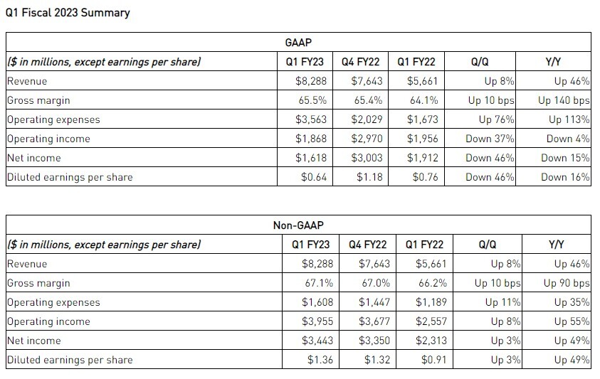
NVIDIA (NASDAQ: NVDA) today reported record revenue for the first quarter ended May 1, 2022, of $8.29 billion, up 46% from a year ago and up 8% from the previous quarter, with record revenue in Data Center and Gaming. GAAP earnings per diluted share for the quarter were $0.64, down 16% from a year ago and down 46% from the previous quarter, and include an after-tax impact of $0.52 related to the $1.35 billion Arm acquisition termination charge. Non-GAAP earnings per diluted share were $1.36, up 49% from a year ago and up 3% from the previous quarter.

"We delivered record results in Data Center and Gaming against the backdrop of a challenging macro environment," said Jensen Huang, founder and CEO of NVIDIA. "The effectiveness of deep learning to automate intelligence is driving companies across industries to adopt NVIDIA for AI computing. Data Center has become our largest platform, even as Gaming achieved a record quarter.

Taiwan's Tech Titans Adopt World's First NVIDIA Grace CPU-Powered System Designs

NVIDIA today announced that Taiwan's leading computer makers are set to release the first wave of systems powered by the NVIDIA Grace CPU Superchip and Grace Hopper Superchip for a wide range of workloads spanning digital twins, AI, high performance computing, cloud graphics and gaming. Dozens of server models from ASUS, Foxconn Industrial Internet, GIGABYTE, QCT, Supermicro and Wiwynn are expected starting in the first half of 2023. The Grace-powered systems will join x86 and other Arm-based servers to offer customers a broad range of choice for achieving high performance and efficiency in their data centers.

"A new type of data center is emerging—AI factories that process and refine mountains of data to produce intelligence—and NVIDIA is working closely with our Taiwan partners to build the systems that enable this transformation," said Ian Buck, vice president of Hyperscale and HPC at NVIDIA. "These new systems from our partners, powered by our Grace Superchips, will bring the power of accelerated computing to new markets and industries globally."

GIGABYTE Releases Arm-Based Processor Server Supercharged for NVIDIA Baseboard Accelerators

GIGABYTE Technology, an industry leader in high-performance servers and workstations, today announced a new supercharged, scalable server, G492-PD0, that supports an Ampere Altra Max or Altra processor with NVIDIA HGX A100 Tensor Core GPUs for the highest performance in cloud infrastructure, HPC, AI, and more. Leveraging Ampere's Altra Max CPU with a high core count, up to 128 Armv8.2 cores per socket with Arm's M1 core, the G492-PD0 delivers high performance efficiently and with minimized total cost of ownership.

GIGABYTE developed the G492-PD0 in response to a demand for high-performing platform choices beyond x86, namely the Arm-based processor from Ampere. This new G492 server was tailored to handle the performance of NVIDIA's baseboard accelerator without compromising or throttling CPU or GPU performance. This server joins the existing line of GIGABYTE G492 servers that support the NVIDIA HGX A100 8-GPU baseboard on the AMD EPYC platform (G492-ZL2, G492-ZD2, G492-ZD0) and Intel Xeon Scalable (G492-ID0).

NVIDIA Hopper Whitepaper Reveals Key Specs of Monstrous Compute Processor

The NVIDIA GH100 silicon powering the next-generation NVIDIA H100 compute processor is a monstrosity on paper, with an NVIDIA whitepaper published over the weekend revealing its key specifications. NVIDIA is tapping into the most advanced silicon fabrication node currently available from TSMC to build the compute die, which is TSMC N4 (4 nm-class EUV). The H100 features a monolithic silicon surrounded by up to six on-package HBM3 stacks.

The GH100 compute die is built on the 4 nm EUV process, and has a monstrous transistor-count of 80 billion, a nearly 50% increase over the GA100. Interestingly though, at 814 mm², the die-area of the GH100 is less than that of the GA100, with its 826 mm² die built on the 7 nm DUV (TSMC N7) node, all thanks to the transistor-density gains of the 4 nm node over the 7 nm one.

NVIDIA Claims Grace CPU Superchip is 2X Faster Than Intel Ice Lake

When NVIDIA announced its Grace CPU Superchip, the company officially showed its efforts of creating an HPC-oriented processor to compete with Intel and AMD. The Grace CPU Superchip combines two Grace CPU modules that use the NVLink-C2C technology to deliver 144 Arm v9 cores and 1 TB/s of memory bandwidth. Each core is Arm Neoverse N2 Perseus design, configured to achieve the highest throughput and bandwidth. As far as performance is concerned, the only detail NVIDIA provides on its website is the estimated SPECrate 2017_int_base score of over 740. Thanks to the colleges over at Tom's Hardware, we have another performance figure to look at.

NVIDIA has made a slide about comparison with Intel's Ice Lake server processors. One Grace CPU Superchip was compared to two Xeon Platinum 8360Y Ice Lake CPUs configured in a dual-socket server node. The Grace CPU Superchip outperformed the Ice Lake configuration by two times and provided 2.3 times the efficiency in WRF simulation. This HPC application is CPU-bound, allowing the new Grace CPU to show off. This is all thanks to the Arm v9 Neoverse N2 cores pairing efficiently with outstanding performance. NVIDIA made a graph showcasing all HPC applications running on Arm today, with many more to come, which you can see below. Remember that NVIDIA provides this information, so we have to wait for the 2023 launch to see it in action.

NVIDIA Opens NVLink for Custom Silicon Integration

Enabling a new generation of system-level integration in data centers, NVIDIA today announced NVIDIA NVLink -C2C, an ultra-fast chip-to-chip and die-to-die interconnect that will allow custom dies to coherently interconnect to the company's GPUs, CPUs, DPUs, NICs and SOCs. With advanced packaging, NVIDIA NVLink-C2C interconnect would deliver up to 25x more energy efficiency and be 90x more area-efficient than PCIe Gen 5 on NVIDIA chips and enable coherent interconnect bandwidth of 900 gigabytes per second or higher.

"Chiplets and heterogeneous computing are necessary to counter the slowing of Moore's law," said Ian Buck, vice president of Hyperscale Computing at NVIDIA. "We've used our world-class expertise in high-speed interconnects to build uniform, open technology that will help our GPUs, DPUs, NICs, CPUs and SoCs create a new class of integrated products built via chiplets."

NVIDIA Unveils Grace CPU Superchip with 144 Cores and 1 TB/s Bandwidth

NVIDIA has today announced its Grace CPU Superchip, a monstrous design focused on heavy HPC and AI processing workloads. Previously, team green has teased an in-house developed CPU that is supposed to go into servers and create an entirely new segment for the company. Today, we got a more detailed look at the plan with the Grace CPU Superchip. The Superchip package represents a package of two Grace processors, each containing 72 cores. These cores are based on Arm v9 in structure set architecture iteration and two CPUs total for 144 cores in the Superchip module. These cores are surrounded by a now unknown amount of LPDDR5x with ECC memory, running at 1 TB/s total bandwidth.

NVIDIA Grace CPU Superchip uses the NVLink-C2C cache coherent interconnect, which delivers 900 GB/s bandwidth, seven times more than the PCIe 5.0 protocol. The company targets two-fold performance per Watt improvement over today's CPUs and wants to bring efficiency and performance together. We have some preliminary benchmark information provided by NVIDIA. In the SPECrate2017_int_base integer benchmark, the Grace CPU Superchip scores over 740 points, which is just the simulation for now. This means that the performance target is not finalized yet, teasing a higher number in the future. The company expects to ship the Grace CPU Superchip in the first half of 2023, with an already supported ecosystem of software, including NVIDIA RTX, HPC, NVIDIA AI, and NVIDIA Omniverse software stacks and platforms.
NVIDIA Grace CPU Superchip

Supermicro Breakthrough Universal GPU System - Supports All Major CPU, GPU, and Fabric Architectures

Super Micro Computer, Inc. (SMCI), a global leader in enterprise computing, storage, networking solutions, and green computing technology, has announced a revolutionary technology that simplifies large scale GPU deployments and is a future proof design that supports yet to be announced technologies. The Universal GPU server provides the ultimate flexibility in a resource-saving server.

The Universal GPU system architecture combines the latest technologies supporting multiple GPU form factors, CPU choices, storage, and networking options optimized together to deliver uniquely-configured and highly scalable systems. Systems can be optimized for each customer's specific Artificial Intelligence (AI), Machine Learning (ML), and High-Performance Computing (HPC) applications. Organizations worldwide are demanding new options for their next generation of computing environments, which have the thermal headroom for the next generation of CPUs and GPUs.

NVIDIA and Global Partners Launch New HGX A100 Systems to Accelerate Industrial AI and HPC

NVIDIA today announced it is turbocharging the NVIDIA HGX AI supercomputing platform with new technologies that fuse AI with high performance computing, making supercomputing more useful to a growing number of industries.

To accelerate the new era of industrial AI and HPC, NVIDIA has added three key technologies to its HGX platform: the NVIDIA A100 80 GB PCIe GPU, NVIDIA NDR 400G InfiniBand networking, and NVIDIA Magnum IO GPUDirect Storage software. Together, they provide the extreme performance to enable industrial HPC innovation.

NVIDIA Announces Grace CPU for Giant AI and High Performance Computing Workloads

NVIDIA today announced its first data center CPU, an Arm-based processor that will deliver 10x the performance of today's fastest servers on the most complex AI and high performance computing workloads.

The result of more than 10,000 engineering years of work, the NVIDIA Grace CPU is designed to address the computing requirements for the world's most advanced applications—including natural language processing, recommender systems and AI supercomputing—that analyze enormous datasets requiring both ultra-fast compute performance and massive memory. It combines energy-efficient Arm CPU cores with an innovative low-power memory subsystem to deliver high performance with great efficiency.

GIGABYTE Releases 2U Server: G262-ZR0 with NVIDIA HGX A100 4-GPU

GIGABYTE Technology, (TWSE: 2376), an industry leader in high-performance servers and workstations, today announced the G262-ZR0 for HPC, AI, and data analytics. Designed to support the highest-level of performance in GPU computing, the G262-ZR0 incorporates fast PCIe 4.0 throughput in addition to NVIDIA HGX technologies and NVIDIA NVLink to provide industry leading bandwidth performance.

NVIDIA is Preparing Co-Packaged Photonics for NVLink

During its GPU Technology Conference (GTC) in China, Mr. Bill Dally—NVIDIA's chief scientist and SVP of research—has presented many interesting things about how the company plans to push the future of HPC, AI, graphics, healthcare, and edge computing. Mr. Dally has presented NVIDIA's research efforts and what is the future vision for its products. Among one of the most interesting things presented was a plan to ditch the standard electrical data transfer and use the speed of light to scale and advance node communication. The new technology utilizing optical data transfer is supposed to bring the power required to transfer by a significant amount.

The proposed plan by the company is to use an optical NVLink equivalent. While the current NVLink 2.0 chip uses eight pico Joules per bit (8 pJ/b) and can send signals only to 0.3 meters without any repeaters, the optical replacement is capable of sending data anywhere from 20 to 100 meters while consuming half the power (4 pJ/b). NVIDIA has conceptualized a system with four GPUs in a tray, all of which are connected by light. To power such a setup, there are lasers that produce 8-10 wavelengths. These wavelengths are modulated onto this at a speed of 25 Gbit/s per wavelength, using ring resonators. On the receiving side, ring photodetectors are used to pick up the wavelength and send it to the photodetector. This technique ensures fast data transfer capable of long distances.

NVIDIA Announces RTX A6000 48 GB Professional Graphics Card Accelerators

NVIDIA today announced their RTX A6000 series of graphics cards, meant to perform as graphics accelerators for professional workloads. And the announcement marks a big departure for the company's marketing, as the Quadro moniker has apparently been dropped. The RTX A6000 includes all raytracing resources also present on consumer RTX graphics cards, and marks a product segmentation from the company's datacenter-geared A40. The RTXA6000 features a full-blown GA102 chip - meaning 10752 CUDA cores powering single-precision compute performance of up to 38.7 TFLOPs (3.1 TLFOPs higher than that of the GeForce RTX 3090). Besides offering NVIDIA's professional driver support and features, the RTX A6000 features 48 GB of GDDR6 (note the absence of the X) memory - ensuring everything and the kitchen sink can be stored in the cards' VRAM. GDDR6X doesn't currently offer the per-chip density of GDDR6 solution, hence why NVIDIA opted for the lower-performing, yet denser memory variant.

The RTX A6000 features a classic blower-type cooler, and presents a new low-profile NVLink bridge that enables two of them to work in tandem within the same system. NVIDIA vGPU virtualization technologies are supported as well; display outputs are taken care of by 4x DisplayPort connectors, marking the absence of HDMI solutions. The card is currently listed for preorder at a cool and collected $5,500, but with insufficient silicon to offer even to its highest-margin datacenter customers, it remains to be seen exactly how available these will be in the market.

NVIDIA Announces the A100 80GB GPU for AI Supercomputing

NVIDIA today unveiled the NVIDIA A100 80 GB GPU—the latest innovation powering the NVIDIA HGX AI supercomputing platform—with twice the memory of its predecessor, providing researchers and engineers unprecedented speed and performance to unlock the next wave of AI and scientific breakthroughs. The new A100 with HBM2E technology doubles the A100 40 GB GPU's high-bandwidth memory to 80 GB and delivers over 2 terabytes per second of memory bandwidth. This allows data to be fed quickly to A100, the world's fastest data center GPU, enabling researchers to accelerate their applications even faster and take on even larger models and datasets.

"Achieving state-of-the-art results in HPC and AI research requires building the biggest models, but these demand more memory capacity and bandwidth than ever before," said Bryan Catanzaro, vice president of applied deep learning research at NVIDIA. "The A100 80 GB GPU provides double the memory of its predecessor, which was introduced just six months ago, and breaks the 2 TB per second barrier, enabling researchers to tackle the world's most important scientific and big data challenges."

GIGABYTE Intros GeForce RTX 3090 VISION OC Graphics Card

GIGABYTE backed up its late September launch of the RTX 3080-based VISION OC graphics card targeted at creators, with one based on the GeForce RTX 3090 (model: GV-N3090VISION OC-24GD), a GPU that offers greater dividends to creators thanks to its 24 GB video memory. GIGABYTE's VISION brand of graphics cards and motherboards are targeted at creators, and the RTX 3090 VISION OC, when paired with NVIDIA's GeForce Studio drivers, provides a formidable solution halfway between the gaming and professional-visualization market segments.

The GIGABYTE RTX 3090 VISION OC comes with the same board design as the RTX 3080 VISION OC, but with the addition of the NVLink interface for explicit multi-GPU. The card comes with a mild factory-OC which sees the GPU boost up to 1755 MHz (vs. 1695 MHz reference), while the memory is left untouched at 19.5 Gbps (GDDR6X-effective), for 940 GB/s of memory bandwidth. Display interfaces include three DisplayPort 1.4a and two HDMI 2.1 connectors. The card draws power from two 8-pin PCIe power connectors. It uses a triple-slot, triple-fan cooling solution with the VISION design scheme. The company didn't reveal pricing.

NVIDIA Unveils RTX A6000 "Ampere" Professional Graphics Card and A40 vGPU

NVIDIA today unveiled its RTX A6000 professional graphics card, the first professional visualization-segment product based on its "Ampere" graphics architecture. With this, the company appears to be deviating from the Quadro brand for the graphics card, while several software-side features retain the brand. The card is based on the same 8 nm "GA102" silicon as the GeForce RTX 3080, but configured differently. For starters, it gets a mammoth 48 GB of GDDR6 memory across the chip's 384-bit wide memory interface, along with ECC support.

The company did not reveal the GPU's CUDA core count, but mentioned that the card's typical board power is 300 W. The card also gets NVLink support, letting you pair up to two A6000 cards for explicit multi-GPU. It also supports GPU virtualization, including NVIDIA GRID, NVIDIA Quadro Virtual Data Center Workstation, and NVIDIA Virtual Compute Server. The card features a conventional lateral blower-type cooling solution, and its most fascinating aspect is its power input configuration, with just the one 8-pin EPS power input. We will update this story with more information as it trickles out.
Update 13:37 UTC: The company also unveiled the A40, a headless professional-visualization graphics card dedicated for virtual-GPU/cloud-GPU applications (deployments at scale in data-centers). The card has similar specs to the RTX A6000.

Update 13:42 UTC: NVIDIA website says that both the A40 and RTX A6000 a 4+4 pin EPS connector (and not 8-pin PCIe) for power input. An 8-pin EPS connector is capable of delivering up to 336 W (4x 7 A @ 12 V).

NVIDIA's Ampere-based Quadro RTX Graphics Card Pictured

Here is the first picture of an alleged next-generation Quadro RTX graphics card based on the "Ampere" architecture, courtesy YouTube channel "Moore's Law is Dead." The new Quadro RTX 6000-series shares many of its underpinnings with the recently launched GeForce RTX 3080 and RTX 3090, in being based on the 8 nm "GA102" silicon. The reference board design retains a lateral blower-type cooling solution, with the blower drawing in air from both sides of the card, through holes punched in the PCB, "Fermi" style. The card features the latest NVLink bridge connector, and unless we're mistaken, it features a single power input near its tail end, which is very likely a 12-pin Molex MicroFit 3.0 input.

As for specifications, "Moore's Law is Dead," shared a handful of alleged specifications that include maxing out of the "GA102" silicon, with all its 42 TPCs (84 SMs) enabled, working out to 10,752 CUDA cores. As detailed in an older story about the next-gen Quadro, NVIDIA is prioritizing memory size over bandwidth, which means this card will receive 48 GB of conventional 16 Gbps GDDR6 memory across the GPU's 384-bit wide memory interface. The 48 GB is achieved using twenty four 16 Gbit GDDR6 memory chips (two chips per 32-bit wide data-path). This configuration provides 768 GB/s of memory bandwidth, which is only 8 GB/s higher than that of the GeForce RTX 3080. The release date of the next-gen Quadro RTX will depend largely on the supply of 16 Gbit GDDR6 memory chips, with leading memory manufacturers expecting 2021 shipping, unless NVIDIA has secured an early production batch.

NVIDIA Reserves NVLink Support For The RTX 3090

NVIDIA has issued another major blow to multi-GPU gaming with their recent RTX 30 series announcement. The only card to support NVLink SLI in this latest generation will be the RTX 3090 and will require a new NVLink bridge which costs 79 USD. NVIDIA reserved NVLink support for the RTX 2070 Super, RTX 2080 Super, RTX 2080, and RTX 2080 Ti in their Turing range of graphics cards. The AMD CrossFire multi-GPU solution has also become irrelevant after support for it was dropped with RDNA. Developer support for the feature has also declined due to the high cost of implementation, small user base, and often poor performance improvements. With the NVIDIA RTX 3090 set to retail for 1499 USD, the cost of a multi-GPU setup will exceed 3079 USD reserving the feature for only the wealthiest of gamers.

NVIDIA GeForce RTX 3090 "Ampere" Alleged PCB Picture Surfaces

As we are getting close to September 1st, the day NVIDIA launches its upcoming GeForce RTX graphics cards based on Ampere architecture, we are getting even more leaks. Today, an alleged PCB of the NVIDIA's upcoming GeForce RTX 3090 has been pictured and posted on social media. The PCB appears to be a 3rd party design coming from one of NVIDIA's add-in board (AIB) partners - Colorful. The picture is blurred out on the most of the PCB and has Intel CPU covering the GPU die area to hide the information. There are 11 GDDR6X memory modules covering the surrounding of the GPU and being very near it. Another notable difference is the NVLink finger change, as there seems to be the new design present. Check out the screenshot of the Reddit thread and PCB pictures below:
NVIDIA GeForce RTX 3090 PCB NVIDIA GeForce RTX 3090 PCB NVIDIA GeForce RTX 3090 PCB
More pictures follow:

GIGABYTE Announces HPC Systems Powered by NVIDIA A100 Tensor Core GPUs

GIGABYTE, a supplier of high-performance computing (HPC) systems, today disclosed four NVIDIA HGX A100 platforms under development. These platforms will be available with NVIDIA A100 Tensor Core GPUs. NVIDIA A100 is the first elastic, multi-instance GPU that unifies training, inference, HPC, and analytics. These four products include G262 series servers that can hold four NVIDIA A100 GPUs and G492 series that can provide eight A100 GPUs. Each series also distinguishes between two models, which support the 3rd generation Intel Xeon Scalable processor and the 2nd generation AMD EPYC processor. The NVIDIA HGX A100 platform is a key element in the NVIDIA accelerated data center concept that brings huge parallel computing power to customers, thereby helping customers accelerate their digital transformation.

With GPU acceleration becoming the mainstream technology in today's data center. Scientists, researchers and engineers are committed to using GPU-accelerated HPC and artificial intelligence (AI) to meet the important challenges of the current world. The NVIDIA accelerated data center concept, including GIGABYTE high-performance servers with NVIDIA NVSwitch, NVIDIA NVLink, and NVIDIA A100 GPUs, will provide GPU computing power required for different computing scales. The NVIDIA accelerated data center also features NVIDIA Mellanox HDR InfiniBand high-speed networking and NVIDIA Magnum IO software that supports GPUDirect RDMA and GPUDirect Storage.

NVIDIA Tesla A100 "Ampere" AIC (add-in card) Form-Factor Board Pictured

Here's the first picture of a Tesla A100 "Ampere" AIC (add-in card) form-factor board, hot on the heals of the morning big A100 reveal. The AIC card is a bare PCB, which workstation builders will add compatible cooling solutions on. The PCB features the gigantic GA100 processor with its six HBM2E stacks, in the center, surrounded by VRM components, and I/O on three sides. On the bottom side, you will find a conventional PCI-Express 4.0 x16 host interface. Above it, are NVLink fingers. The rear I/O has high-bandwidth network interfaces (likely 200 Gbps InfiniBand), by Mellanox. The tail end has hard points for 12 V power input. Find juicy details of the GA100 in our older article.

NVIDIA Develops Tile-based Multi-GPU Rendering Technique Called CFR

NVIDIA is invested in the development of multi-GPU, specifically SLI over NVLink, and has developed a new multi-GPU rendering technique that appears to be inspired by tile-based rendering. Implemented at a single-GPU level, tile-based rendering has been one of NVIDIA's many secret sauces that improved performance since its "Maxwell" family of GPUs. 3DCenter.org discovered that NVIDIA is working on its multi-GPU avatar, called CFR, which could be short for "checkerboard frame rendering," or "checkered frame rendering." The method is already secretly deployed on current NVIDIA drivers, although not documented for developers to implement.

In CFR, the frame is divided into tiny square tiles, like a checkerboard. Odd-numbered tiles are rendered by one GPU, and even-numbered ones by the other. Unlike AFR (alternate frame rendering), in which each GPU's dedicated memory has a copy of all of the resources needed to render the frame, methods like CFR and SFR (split frame rendering) optimize resource allocation. CFR also purportedly offers lesser micro-stutter than AFR. 3DCenter also detailed the features and requirements of CFR. To begin with, the method is only compatible with DirectX (including DirectX 12, 11, and 10), and not OpenGL or Vulkan. For now it's "Turing" exclusive, since NVLink is required (probably its bandwidth is needed to virtualize the tile buffer). Tools like NVIDIA Profile Inspector allow you to force CFR on provided the other hardware and API requirements are met. It still has many compatibility problems, and remains practically undocumented by NVIDIA.

ZOTAC Announces Its GeForce RTX SUPER Lineup

ZOTAC GAMING is excited to introduce the new GeForce RTX SUPER series of graphics cards pushing more CUDA Cores, more GDDR6 memory, more memory bandwidth, and more power. Continuing the push for next-gen gaming, each SUPER Series enable extraordinary performance with real-time ray tracing with ray tracing cores and tensor cores. Each ZOTAC GAMING GeForce RTX SUPER series is equipped with the most powerful cooling hardware, IceStorm 2.0 cooling, and beautifully lit with SPECTRA lighting.

NVIDIA Brings CUDA to ARM, Enabling New Path to Exascale Supercomputing

NVIDIA today announced its support for Arm CPUs, providing the high performance computing industry a new path to build extremely energy-efficient, AI-enabled exascale supercomputers. NVIDIA is making available to the Arm ecosystem its full stack of AI and HPC software - which accelerates more than 600 HPC applications and all AI frameworks - by year's end. The stack includes all NVIDIA CUDA-X AI and HPC libraries, GPU-accelerated AI frameworks and software development tools such as PGI compilers with OpenACC support and profilers. Once stack optimization is complete, NVIDIA will accelerate all major CPU architectures, including x86, POWER and Arm.

"Supercomputers are the essential instruments of scientific discovery, and achieving exascale supercomputing will dramatically expand the frontier of human knowledge," said Jensen Huang, founder and CEO of NVIDIA. "As traditional compute scaling ends, power will limit all supercomputers. The combination of NVIDIA's CUDA-accelerated computing and Arm's energy-efficient CPU architecture will give the HPC community a boost to exascale."

GIGABYTE Gives AMD X570 the Full Aorus Treatment: ITX to Xtreme

Motherboard vendors are betting big on the success of AMD's "Valhalla" desktop platform that combines a Ryzen 3000-series Zen 2 processor with an AMD X570 chipset motherboard, and have responded with some mighty premium board designs. GIGABYTE deployed its full spectrum of Aorus branding, including Ultra, Elite, ITX Pro, Master, and Xtreme. The X570 I Aorus Pro WiFi mini-ITX motherboard is an impressive feat of engineering despite its designers having to wrestle with the feisty new PCIe gen 4 chipset. It draws power from a combination of 24-pin and 8-pin connectors, and conditions power for the SoC with an impressive 8-phase VRM that uses high-grade PowIRstage components. A rather tall fan-heatsink cools the X570 chipset, with a 30 mm fan.

Connectivity options on the X570 I Aorus Pro WiFi are surprisingly aplenty. The sole expansion slot is a PCI-Express 4.0 x16, but the storage connectivity includes not one, but two M.2-2280 slots (reverse side of the PCB), each with PCI-Express 4.0 x4 and SATA 6 Gbps wiring. Four SATA 6 Gbps ports make for the rest of the storage connectivity. Networking options include 2.4 Gbps 802.11ax WLAN, Bluetooth 5.0 (Intel , and 1 GbE, all pulled by Intel-made controllers. USB connectivity includes six 5 Gbps USB 3.2 gen 1, and two 10 Gbps USB 3.2 gen 2 ports (of which one is type-C), and two 5 Gbps ports by headers. The onboard audio solution has 6-channel analog output, but is backed by a premium Realtek ALC1220VB Enhance CODEC (114 dBA SNR).
Return to Keyword Browsing
May 21st, 2024 11:42 EDT change timezone

New Forum Posts

Popular Reviews

Controversial News Posts