News Posts matching #Roadmap

Return to Keyword Browsing

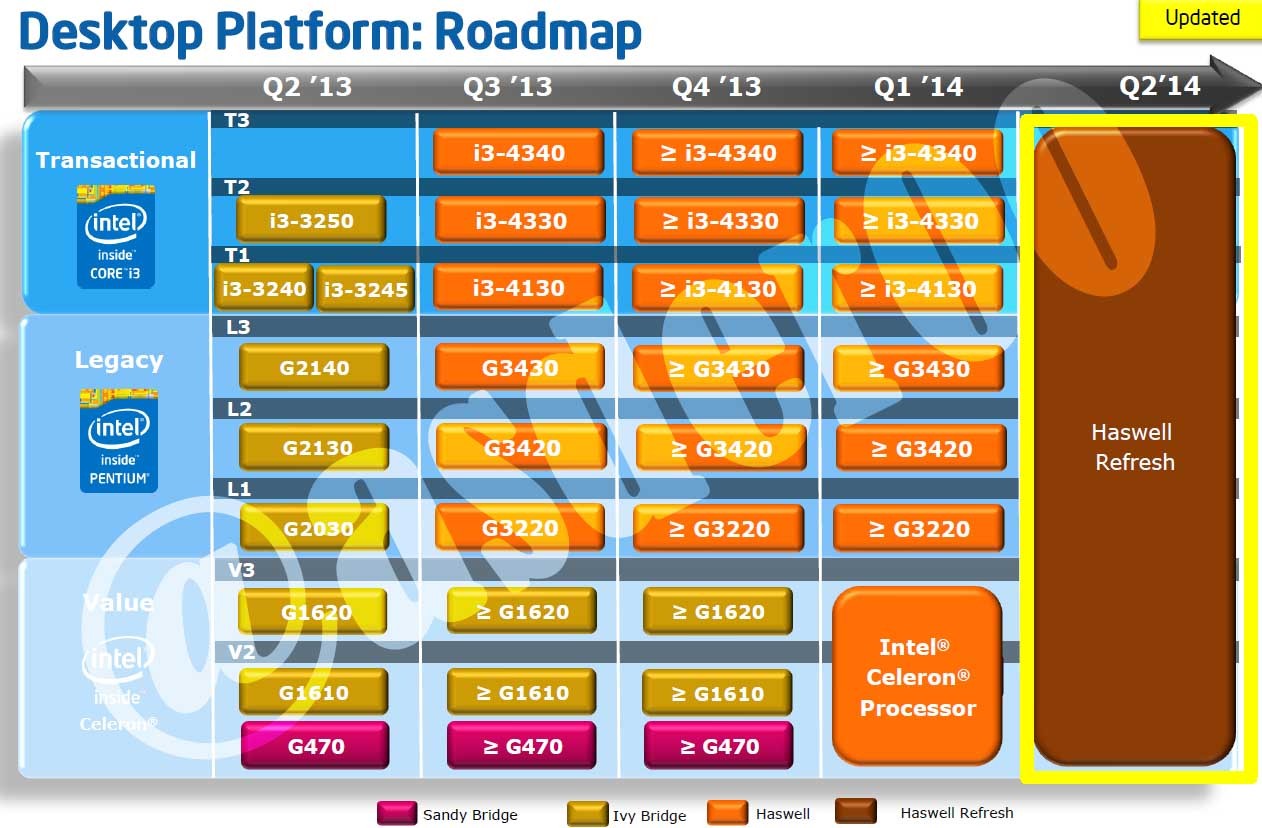
Intel's Desktop Processor Roadmap for H2 2013 to H1 2014 Revealed

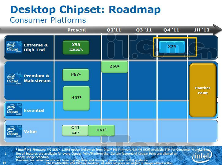
According to CPU World staff, who, by appealing to an unnamed secondary source, managed to confirm the validity of an earlier leak, we are now looking at Intel's desktop roadmap for the following twelve months. The slides reveal the Q3 launch of Intel's Ivy Bridge-E chips, the Core i7-4820K, i7-4930K and i7-4960X comprising the lineup. The new Extreme chips will make use of the existing X79 platform. Also in Q3 the Premium line will receive a new product, the Core i7-4771, which we do not know in what way differs from the currently available Core i7-4770, but a judicious appeal to wild speculation could point out an upgraded IGP.

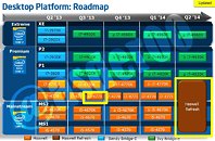
The mid segments will get a platform upgrade in the form of a new H81 chipset, and six new processors, the Core i3-4130, i3-4330, i3-4340, as well as three new Ivy Bridge based Pentium chips, the G3220, G3420 and G3430. Celeron processors are in the pipelines for Q1 2014, while Q2 will follow with the Haswell refresh and the accompanying new platform based on the Z97 and H97 chipsets.

Intel "Ivy Bridge" Celeron and Pentium Processors Priced

Keeping up with an updated launch roadmap for Q1 2013 posted last November, Intel rolled out entry-level Celeron and Pentium dual-core processors based on its 22 nm "Ivy Bridge" silicon. All of the seven desktop and four mobile chips announced occupy price-points under $100. The desktop lineup begins with the Celeron G1610 (2.60 GHz, dual-core, 55W TDP), priced at US $42; Celeron G1610T (2.30 GHz, dual-core, 35W TDP) at $42; followed by Celeron G1620 (2.70 GHz), priced significantly higher at $52; Pentium G2010 (2.80 GHz, dual-core, 55W TDP) and G2020 (2.90 GHz), and G2020T (2.50 GHz, 35W TDP) at $64; and Pentium G2130 (3.20 GHz, dual-core, 55W TDP) at $86.

Intel has two kinds of Celeron mobile processors, targeting the mainstream and Ultrabook-like notebook form-factors. Among the mainstream notebook processors are the Celeron 1000M (1.80 GHz, dual-core, 35W TDP) and Celeron 1020M (2.10 GHz, dual-core, 35W TDP). Among the Ultrabook-like form-factor models are the Celeron 1007U (1.50 GHz, dual-core, 17W TDP), and Celeron 1037U (1.80 GHz, dual-core, 17W TDP). Interestingly, all four mobile Celeron "Ivy Bridge" CPU models are priced at $86, in 1000-unit tray quantities.

Ethernet Alliance Executives Outline Roadmap for Continued Ethernet Evolution

The Ethernet Alliance, a global consortium dedicated to the continued success and advancement of Ethernet technologies, today announced Chairman, John D'Ambrosia of Dell, and Marketing Committee Chair, Chauncey Schwartz of QLogic, will be featured speakers at the upcoming Large Installation System Administration Conference (LISA '12). A technical educational conference and networking event for system administrators of all levels of expertise, LISA '12 is scheduled for December 9 - 14, 2012 at San Diego, CA's Sheraton San Diego Hotel & Marina.

Ethernet is at the next critical junction in its lifecycle, particularly with the emergence of new applications like cloud computing and server virtualization, that could profoundly impact this essential technology," said John D'Ambrosia, chairman, Ethernet Alliance, and chief Ethernet evangelist, CTO office, Dell. "Therefore, it's important to understand the current conditions within the Ethernet ecosystem, as well as taking a forward-facing view of where we'll be six months, a year, or even five years down the road."

Intel Updates CPU Launch Roadmap for Q1 2013

With the dawn of 2013, and no catastrophes in sight, Intel is going ahead with its usual business of phasing out old processor models, and making way for new ones. By the end of 2012, Intel will stop taking orders for several processor models mostly based on the older 32 nm "Sandy Bridge" silicon. These include chips such as the Core i7-2700K, Core i5-2310, Core i3-2105, Pentium G440, and surprisingly, an early demise of the 22 nm Core i5-3450, which is cannibalized by the Core i5-3470 at the same price point. Pentium G870, G645 and G645T as well as Celeron G555, G550 and G550T are the other chips on the chopping block.

Come 2013, Intel will release Pentium and Celeron series processors based on its 22 nm "Ivy Bridge" micro-architecture. These include the Pentium G2130, G2020 and G2020T and Celeron G1620, G1610 and G1610T. In the mobile (notebook) CPU sphere, Intel will launch dual-core "Ivy Bridge" chips to layer out its Ultrabook product segment. These include the Core i7-3687, Core i5-3437U, Celeron 1037U, 1007U, 1020M and 1000M. In March, the company is expected to launch its 4th generation Core "Haswell" line of processors.

Production of AMD "Piledriver" FX Processors Begin Q3 2012

Production of AMD's next-generation FX processor family, which are based on its "Piledriver" microarchitecture, will commence in Q3 2012, according to industry sources. Some of the first client processor models based on the "Vishera" silicon, will be the eight-core FX-8350, six-core FX-6300, and quad-core FX-4320. The three model names were earlier misinterpreted with an "x" prefix from a roadmap slide.

A few more details are known about these chips. For starters, the chips will be built on the existing AM3+ package, retaining compatibility with current AM3+ platforms. The chips will also retain dual-channel DDR3-1866 MHz integrated memory controllers, and Turbo Core 2.0. The main differences here, are increases in IPC (performance to clock-speed ratio), and the implementation of resonant clock mesh technology, which increases energy efficiency.

Ivy Bridge Desktop Core i3 Processor Lineup Detailed, Lack PCIe Gen. 3.0

Details of desktop Core i7 and Core i5 "Ivy Bridge" processors in the LGA1155 package have been detailed at lengths, in the past. Core i3 parts based on the same 22 nm Ivy Bridge silicon, however, were relatively known. Tables listing out updated information about the lineup points out that Intel has as many as five Core i3 "Ivy Bridge" desktop processors in the works, all dual-core, and among which two are low-power parts.

The table also suggests that these Core i3 chips will have reduced features, importantly, the lack of PCI-Express 3.0 bus. When connected to these chips, PCI-E 3.0 add-on cards (such as graphics cards) will function in PCI-Express 2.0 mode. Further, these chips will lack support for AES-NI (accelerates encryption), VT-d (enhanced virtualization), and TXT (security). Certain models in the lineup have faster integrated graphics, denoted by a "5" in the end of the model number. These chips also lack Turbo Boost for the x86 cores, but feature HyperThreading.

AMD "Trinity" APU Models Further Detailed

In the second quarter of this year, AMD will launch its next-generation accelerated processing unit, codenamed "Trinity", starting with quad-core A10 and A8 parts in the quarter, followed by dual-core A6 and A4 parts in the third-quarter of 2012 (more here). DonanimHaber scored a specifications-sheet that details all the models AMD has in store for this year, also giving us an insight to what constitute each of these model numbers.

An interesting revelation here is that AMD does not have triple-core APUs anywhere in its lineup. The A10 lineup consists of quad-core APUs that come with Radeon HD 7660D graphics, while the A8 lineup also consists of quad-core APUs, but with slower Radeon HD 7560D graphics. The A6 lineup consists of dual-core APUs with Radeon HD 7540D graphics, while the A4 lineup has dual-core APUs with Radeon HD 7480D graphics.

AMD 2012 CPU Roadmap Unveils FX-X300 and A10 Series

AMD is pushing on with a desktop product lineup that's leveraging its Piledriver CPU and Graphics CoreNext GPU architectures in 2012. Apparently, the company will have a faster product development cycle to catch up with Intel's "Tick-Tock", as revealed in a roadmap slide scored by DonanimHaber. The current product lineup will remain unchanged in the first quarter of 2012. Then in the second quarter, AMD will launch a few more socket AM3+ FX-8000, FX-6000, and FX-4000 series eight, six, and four-core processors; along with the much talked about "Trinity" accelerated processing unit.

The fastest "Trinity" APUs will get a new brand identifier, the A10-5000 series. These APUs will pack next-generation "Piledriver" modular cores and Radeon HD 7600D series graphics. Around this time, AMD will also launch the Brazos 2.0 low-power APU for netbooks, nettops, and embedded computing devices. Brazos 2.0 will get the E2-1000 series branding. The big change is reserved for the third quarter of 2012, when AMD launches the successor of its less-than-lucky AMD FX "Bulldozer" processor family.

AMD Strategy Transformation Brings Agile Delivery of Industry-Leading IP

At its annual Financial Analyst Day, AMD (NYSE: AMD) detailed a new "ambidextrous" strategy that builds on the company's long history of x86 and graphics innovation while embracing other technologies and intellectual property to deliver differentiated products.

AMD is adopting an SoC-centric roadmap designed to speed time-to-market, drive sustained execution, and enable the development of more tailored customer solutions. SoC design methodology is advantageous because it is a modular approach to processor design, leveraging best practice tools and microprocessor design flows with the ability to easily re-use IP and design blocks across a range of products.

AMD Outlines Its 2012-2013 Client Roadmap, Big Focus is on APUs

Today at its annual Financial Analyst Day, AMD has presented an updated roadmap detailing the hardware it plans to bring to the table during 2012 and 2013. For this year, the Sunnyvale-based company is preparing a processor quarter which includes the Trinity, Brazos 2.0 and Hondo APUs (accelerated processing units) and the Vishera CPU.

Set to be the main weapon in AMD's x86 arsenal, the Trinity APU (aka the 2nd gen A Series) is made on 32 nm process technology, and features DirectX 11 graphics, two/four Piledriver cores (Piledrive is said to deliver 25% better performance than the Stars cores found in Llano APUs), and a TDP that can go as low as 17 W on mobile parts. Trinity is expected to debut in Q2 and already has close to 100 design wins (more than Llano had before its release).

Intel 'Ivy Bridge' Core Desktop Processor Prices Compiled

In 2012, Intel will update its processor lineup up to performance 2 tiers with new models based on the spanking new 22 nm "Ivy Bridge" silicon, which will increase performance over the current generation, and bring some new features to the table. In late November, a list of desktop Core i5/i7 models could be compiled, which were later confirmed on roadmap slides. CPU World compiled retail channel pricing of several of those Core i5/i7 "Ivy Bridge" chips. The prices look to be more or less consistent with current "Sandy Bridge" Core processors, which those chips are bound to replace. The Core i7-3770K, for example, which will replace the Core i7-2600K, will be similarly priced to it.

Intel 2012 Core Processor Model Names Confirmed on Roadmap Slide

Earlier this week, a report tabled the model numbers of Intel's 2012 Core processor family based on the "Ivy Bridge" silicon. Its processor model number scheme consisted of Core i5/i7 3000 series, targeting various market price points. Many of these model numbers are confirmed on the latest roadmap slide detailing the Core processor family for 2012. We are also getting to see what the nomenclature of next-generation Core i3 processors could look like.

The slide shows that Ivy Bridge processors will start selling in Q2 2012, which is consistent with reports of an April 2012 launch. Intel will begin with Core i3-32xx (xx = TBD), i5-3450, i5-3550, i5-3570K, i7-3770, and i7-3770K. Around this time, there will be a market transition among cheaper Core i3 parts. In Q3 2012, i5-3470 and i5-3570 will displace i5-3450 and i5-3550; while a faster Core i7-37x0K processor will displace the i7-3770K. The market transition among some Core i3 parts will continue in Q3. Q4 2012 will largely resemble Q3, except that the lower-end Core i3 lineup will have fully transitioned to Ivy Bridge. There will be no changes in the LGA2011 Sandy Bridge-E HEDT lineup, except that an affordable quad-core part will be added in Q1 2012. For quick reference, we re-posted the table from the older report.

NVIDIA GeForce Kepler Roadmap Compiled

2012-13 promises to be a period of big graphics product launches, centric to a new DirectX version, DirectX 11.1, which will ship with Microsoft's next major Windows version (currently referred to as Windows 8). Information compiled by ExpertsPC.com and 4Gamer.net tables what NVIDIA's next-generation graphics family could look like, and around what time it could be released to market. With its next-generation GeForce Kepler family of GPUs, NVIDIA will follow a sensible bottom-up product release model, to ensure that it isn't met with any technical hurdles with TSMC's new 28 nm manufacturing process, and so it could launch GPUs with increasingly higher transistor counts, till its top-of-the-line GPU is outed.

The first GPU in NVIDIA's pipeline is the GeForce Kepler 107 (GK107), on which will be based entry thru lower-mainstream SKUs. The data doesn't reveal things like core counts, but points out that GK107 will have a 128-bit wide GDDR5 memory interface, will use the current-generation PCI-Express 2.0 bus, will be built on the 28 nm process, and will support DirectX 11.1. This will be followed by the GK106, on which "sweet-spot" SKUs could be based. This will be NVIDIA's first PCI-Express 3.0 compliant GPU, it will have a 256-bit wide GDDR5 memory interface.

Sandy Bridge-E Model Numbers, Clock Speeds Surface

Here are details of the first three models of Intel's "Sandy Bridge-E" Core i7 processors in the LGA2011 package. Some of these details were made public as early as mid-April. It was then analyzed that Intel was driving two distinct lines of LGA2011 client processors: Enthusiast and Performance, and within Performance, there were BClk multiplier-unlocked six-core, and locked quad-core chips. With the new series, Intel will move to the 3000 series of processor model numbering, indicating that the new processors will be part of Intel's 3rd generation Core processors, even though they're based on the Sandy Bridge architecture.

Before we move to the model numbers, here's a quick run up of the brand extenders. "X" denotes Extreme Edition, "K" denotes "Unlocked" (BClk multipler unlocked). Leading the pack will be Core i7-3960X Extreme Edition. This six-core (6 cores, 12 threads with HTT) chip has a nominal clock speed of 3.30 GHz, Turbo Boost speed of up to 3.90 GHz, and features the full 15 MB of L3 cache present on the Sandy Bridge-E silicon. Expect this chip to have a four figure price-tag.

Sandy Bridge-E Delayed to January 2012: Sources

Originally slated for Q4 2011, the launch of Intel's Sandy Bridge-E desktop/workstation platform has been pushed back to Q1 2012, sources told VR-Zone. The high-end platform was expected by industry observers to be a December launch, targeting the shopping season, but it seems like January 2012 is found to be more fitting. Perhaps the International CES, where the latest and greatest from the tech industry is unveiled, serves as the ideal launch-pad for Sandy Bridge-E.

Sandy Bridge-E is an upscale of the architecture that makes up Intel's 2011 Core processor family. Consisting of 4 or 6 cores, Sandy Bridge makes up two distinct product lines for the client desktop market. The chips pack massive quad-channel DDR3 integrated memory controllers and PCI-Express 3.0 hubs that can drive up to four graphics cards. The processor is made of a new 2011-pin LGA package, with the new Intel X79 chipset handling the rest of the platform.

Gigabyte X79 UD3 LGA2011 Motherboard First Shot

Here is the first picture of GA-X79A-UD3, the first Gigabyte-branded socket LGA2011 motherboard. Based on the Intel X79 Express chipset, the board supports upcoming Sandy Bridge-E enthusiast processors in the LGA2011 package. Mind you, this is just the cheapest LGA2011 board from Gigabyte, there is a higher-end line of X79 motherboards, so don't let the unspectacular looks of the UD3 get you.

The GA-X79A-UD3 is a standard ATX sized motherboard. Its main VRM is spread all around the large CPU socket, in what appears to be a 6-phase design, with an unknown number of memory and uncore phases. LGA2011 processors feature a large quad-channel DDR3 memory controller, along with a northbridge uncore component with a 40-lane PCI-Express 3.0 controller. Those amount to the socket's insane pin-count of 2,011 pins. Memory slots are located in pairs of two on either sides of the socket. Each slot is its own 64-bit wide memory channel.

Computex 2011 Launchpad for Intel X79 Motherboards

At Computex 2010, motherboard vendors across the board displayed socket LGA1155 motherboards that support Intel "Sandy Bridge" processors, based on P67, H67 chipsets, months in advance of the platform actually making it to the market. This year, the motherboard industry will do something similar and show off socket LGA2011 motherboards based on the Intel X79 "Patsburg" chipset.

Detailed to much length in older articles, the platform schematic of Sandy Bridge-E surfaced, confirming X79's feature-set, including a PCI-Express 3.0 based supplementary interconnect between the processor and chipset to bolster enough bandwidth for the massive 10-port SATA 6 Gb/s controller, and a 8-port PCI-Express 2.0 hub. Sandy Bridge-E processor itself comes in three main variants, an all-enabled 6-core Extreme Edition, a 6-core unlocked variant, and a limited-OC 4-core variant. The platform is slated for late 2011.

Leaked Roadmap Reveals Two Lines of Enthusiast Sandy Bridge-E Processors

In Q4 2011, Intel will unveil its new Sandy Bridge-E (enthusiast) platform, consisting of new multi-core processors in the 2011-pin LGA package, and Intel X79 Express chipset. A roadmap slide leaked to the Chinese media reveals an interesting way in which Intel will approach the platform to monetize it best. To begin with, it appears like Sandy Bridge-E will keep up with the trend set by LGA1155 processors where only certain models can be overclocked, while others are greatly limited. Among those that can be overclocked (or "unlocked", as Intel puts it,) there will be two classes.

The first class are the 6-core chips at the very top of the pile, probably branded "Extreme Edition", which feature both unlocked BClk multipliers, and have 15 MB of L3 cache, among several other features enabled. Traditionally these processors cost around US $1000. The first of such chips will be clocked at 3.30 GHz. The second class of "unlocked" chips are those which make overclocking more accessible at lower price points (we're thinking under $600), probably branded with the "K" brand identifier extension (eg: 2600K). These 6-core chips will feature unlocked multipliers, while having 12 MB of cache enabled. The first of these chips will be clocked at 3.20 GHz.

Intel X79 Enthusiast Chipset Sketched in Roadmap

Intel's next platform for enthusiasts (successor to LGA1366, X58), will consist of a 2011-pin LGA socket, the Sandy Bridge-E (enthusiast) processor that features a massive quad-channel DDR3 memory controller and 32+ lane PCI-Express 2.0 hub, and the X79 chipset. Intel is looking to skip the 6-series chipset family with its next high-end platform chipset, and perhaps it makes sense since the platform is slated for Q4 2011. The X79 is a PCH (platform controller hub), like P55 and P67, since Intel has reorganized the platform. The beefy PCI-E hub housed in the X58 northbridge is relocated to the processor die, and the southbridge is given a much needed overhaul in terms of connectivity.

The X79 is much bigger than P67 in terms of connectivity and features. Differences start right at the interconnect. While P67 connects to the processor over DMI (physical PCI-Express 2.0 x4), X79 supplements this link with an additional PCI-Express 2.0 x4 link to the processor's PCI-E hub if the user chooses so, in the EFI setup program. The chipset bus hence ends up with 8 GB/s of bandwidth, and wait till you hear what will make use of it: a 10-port SATA 6 Gb/s RAID controller integrated to the PCH! That is a huge improvement in terms of storage connectivity, which is limping with 2-port SATA 6 Gb/s (next to four 3 Gb/s ports) on 6-series chipsets.

AMD Zambezi ''Bulldozer'' Desktop CPU Roadmap Revealed

AMD's next-generation PC processor architecture that seeks to challenge the best Intel has, codenamed "Bulldozer", is set to make its desktop PC debut in 2Q next year, with a desktop processor die codenamed "Zambezi". AMD is seeking to target all market segments, including an enthusiast-grade 8-core segment, a performance 6-core segment, and a mainstream 4-core segment. The roadmap reveals that Zambezi will make its entry with the enthusiast-grade 8-core models first, starting with 125W and 95W models, trailed by 6-core and 4-core ones.

Another couple of architectural details revealed is that Zambezi's integrated memory controller (IMC) supports DDR3-1866 MHz as its standard memory type, just like Deneb supports DDR3-1333 MHz as its standard. DDR3-1866 MHz, or PC3-14900 as it's technically known, will churn out 29.8 GB/s in dual-channel mode, that's higher than triple-channel DDR3-1066 MHz (25.6 GB/s), which is Intel Core i7 LGA1366 processors' official memory standard. The 8-core and 6-core Zambezi models feature 8 MB of L3 cache, while the 4-core ones feature 4 MB. Another tidbit you probably already knew is that existing socket AM3 processors are forwards-compatible with AM3+ (Zambezi's socket), but Zambezi processors won't work on older AM3/AM2(+) socket motherboards.

AMD Details a Vivid Future of Computing at Annual Financial Analyst Day

At its annual Financial Analyst Day, AMD (NYSE: AMD) demonstrated how its unique combination of CPU and GPU computing technologies on a single die will enable breakthrough capabilities in an innovative processor design with planned OEM system availability in early 2011. AMD executives detailed how this new class of processor, AMD Fusion Accelerated Processing Units (APUs), is poised to create a sustained position of advantage by powering demanding PC workloads in sleek form factors with long battery life, pacing future AMD growth. AMD Fusion APUs are built from DirectX 11-capable GPU technology and either low-power or high-performance multi-core x86 CPU technology. These APUs are designed to vastly improve today's Internet, video processing and playback, and gaming (client and online) experiences. For the first time, AMD also demonstrated its new high-performance x86 multi-core CPU architecture codenamed "Bulldozer" and provided additional information around the "Bulldozer" launch schedule.

PC DDR4-SDRAM Surfaces on JEDEC Roadmaps

PC DDR4-SDRAM, the successor standard for DDR3-SDRAM, which continues increasing memory bandwidths while maintaining the same electrical footprints, surfaced on JEDEC roadmaps, at a recent MemCon conference in Tokyo, Japan. Just the target clock speed range for DDR2-SDRAM was 400~1066 MHz, and that of DDR3-SDRAM is 1066~2133 MHz, the DDR4-SDRAM standard will aim for clock speeds between 2133 and 4266 MHz, with DRAM voltages of 1.1~1.2V, the voltages standards-compliant DDR3 memory will ultimately end up with. Some of the first DDR4 memory chips will be built on the 32 nm or 36 nm manufacturing processes. JEDEC expects sampling of the new memory type to start in 2011 for the industry to come up with appropriate memory controllers and deployment platforms, while actual mass production is slated by 2015.

Intel 2011 Core Series Desktop Processor Roadmap Surfaces

Having turned its most profitable quarter, Intel is banking on its vast lineup of the 2010 Core processors, which will be updated towards the end of the year. By 2011, Intel will have a new series of second generation Core i7, Core i5, and Core i3 processors, based on a brand new architecture, and built for new sockets and chipsets. A roadmap of the same reached sections of the European media, which shows the company to be almost ready with a full-fledged lineup of desktop processors covering most price-points, by 2011.

The new architecture on which these processors are based is referred to by Intel as "Sandy Bridge", key features of which include the inclusion of the new Advanced Vector Extensions (AVX), a more advanced instruction set than SSE, to accelerate complex applications. AVX aside, there's Turbo Boost technology 2.0 that comes with even smarter algorithms to automatically manage clock speeds of individual processor cores to maximize performance within the processor's TDP envelope, AES-NI, which is a more manageable hardware data encryption instruction set, and processors with integrated graphics (IGP) controllers will have even faster ones, because Intel will be relocating the IGP and memory controller to the same die as the processor cores, this IGP is referred to as Intel "GT2" graphics.

New Roadmap Shows AMD's Desktop Processor Portfolio for Rest of 2010

A set of new slides by AMD to sections of the industry spills the beans on AMD's processor offer outlook for perhaps the rest of the year. It shows AMD to maintain focus on value-oriented models that etch away Intel's market share on grounds of price/performance, while the higher-end of the spectrum keeps up with the latest technologies including the industry-wide advent of the six-core processor era, as well as new power-state management technologies such as TurboCore, which steps up clock speeds of certain cores of the processors while powering down others, which the load is low or less-parallel.

Front-line processor lineups include the Phenom II X6, and Phenom II X4, including a new T X4 series that includes TurboCore support. AMD's transition towards these chips from the existing Deneb-based quad-core ones starts within this quarter lasting throughout Q2 and part of Q3 2010. It includes Phenom II X4 960T, a 3.00 GHz (3.40 GHz turbo) chip based on the Zosma die. It goes up with the Phenom II X6 1035T, a six-core chip clocked at 2.60 GHz (3.10 GHz turbo). A notch higher up is the Phenom II X6 1055T, clocked at 2.80 GHz (3.30 GHz turbo), which comes in 95W and 125W variants. At the top is the Phenom II X6 1090T Black Edition, an overclocker-friendly chip that runs at 3.20 GHz (3.60 GHz turbo). A little later in Q3, AMD will add in the Phenom II X6 1075T, clocked at 3.00 GHz (3.50 GHz turbo).

Intel Updates Mainstream, Performance, and Extreme CPU Roadmap

Intel issued a confidential roadmap for CPU product releases that looks as far as Q3 2010, leaked to sections of the Chinese media. The roadmap covers prominent Intel processors in their designated market segments drawn out by Intel, covering three grades of mainstream, one each of performance and extreme. The roadmap marks a definite transition of architectures from Intel's Core (penryn) to next-generation Nehalem, and the advent of Intel's first 32 nm based Westmere CPUs.

To begin with, there three models of Intel's first LGA-1156 processors scheduled for Q3 2009, the quad-core "Lynnfield" based Core i7 870 (2.93 GHz, HTT) in Performance, Core i7 860 (2.80 GHz, HTT) in MS3/upper-mainstream, and Core i5 750 (2.66 GHz, no HTT) in MS2/middle-mainstream. The HTT-enabled Core i7 800 processors were earlier believed to have been scheduled for Q1 2010, but are combined with the Core i5 750 for a grand platform launch. The Core i7 800 models will remain seated in their segments for the better part of 2010.
Return to Keyword Browsing
Jul 5th, 2025 23:15 CDT change timezone

New Forum Posts

Popular Reviews

TPU on YouTube

Controversial News Posts