News Posts matching #Wafer

Return to Keyword Browsing

TrendForce: Demand for Consumer Electronics Sluggish, NAND Flash Wafer Pricing Leads Downturn in May

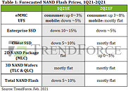
According to TrendForce research, looking at NAND Flash wafers, the pricing of which more sensitively reflects the market, suppliers are increasingly motivated to cut prices in exchange for sales due to weak retail demand since March and a more conservative outlook for shipments of other end products. The price of NAND Flash wafers is expected to begin falling in May and the supply of NAND Flash will gradually overtake demand in 2H22. The price decline of NAND Flash wafers in 3Q22 may reach 5~10%.

At the same time, TrendForce indicates that February's contamination incident at Kioxia was expected to tighten the market in 2Q22 and 3Q22. However, as a consequence of rising inflation and the war between Russia and Ukraine, market demand for consumer products in the traditional peak season of the second half of the year is trending conservative and the prices of client SSD, eMMC, and UFS in 3Q22 will be flat compared to 2Q22, breaking from the original expectation that prices may rise. In terms of enterprise SSDs, as demand for data centers remains strong, no significant correction in demand has yet been observed. However, as the overall NAND Flash market gradually moves into oversupply, prices will only grow slightly by approximately 0~5% in 3Q22.

UMC Announces New 22nm Wafer Fab in Singapore

United Microelectronics Corporation ("UMC" or "The Company"), a leading global semiconductor foundry, today announced that its Board of Directors has approved a plan to build a new advanced manufacturing facility next to its existing 300 mm fab (Fab12i) in Singapore. The first phase of this greenfield fab will have a monthly capacity of 30,000 wafers with production expected to commence in late 2024.

The new fab (Fab12i P3) will be one of the most advanced semiconductor foundries in Singapore, providing UMC's 22/28 nm processes. The planned investment for this project will be US$5 billion. UMC has operated as a pure-play foundry supplier in Singapore for more than 20 years and the location is also the company's designated R&D center for advanced specialty technologies. To account for the Fab12i expansion, the company's 2022 capex budget will be revised upward to US$3.6 billion.

8-inch Wafer Capacity Remains Tight, Shortages Expected to Ease in 2H23, Says TrendForce

From 2020 to 2025, the compound annual growth rate (CAGR) of 12-inch equivalent wafer capacity at the world's top ten foundries will be approximately 10% with the majority of these companies focusing on 12-inch capacity expansion, which will see a CAGR of approximately 13.2%, according to TrendForce's research. In terms of 8-inch wafers, due to factors such as difficult to obtain equipment and whether capacity expansion is cost-effective, most fabs can only expand production slightly by means of capacity optimization, equating to a CAGR of only 3.3%. In terms of demand, the products primarily derived from 8-inch wafers, PMIC and Power Discrete, are driven by demand for electric vehicles, 5G smartphones, and servers. Stocking momentum has not fallen off, resulting in a serious shortage of 8-inch wafer production capacity that has festered since 2H19. Therefore, in order to mitigate competition for 8-inch capacity, a trend of shifting certain products to 12-inch production has gradually emerged. However, if shortages in overall 8-inch capacity is to be effectively alleviated, it is still necessary to wait for a large number of mainstream products to migrate to 12-inch production. The timeframe for this migration is estimated to be close to 2H23 into 2024.

Toshiba to Expand Power Semiconductor Production Capacity With 300-Millimeter Wafer Fabrication Facility

Toshiba Electronic Devices & Storage Corporation ("Toshiba") today announced that it will construct a new 300-milimeter wafer fabrication facility for power semiconductors at its main discrete semiconductor production base, Kaga Toshiba Electronics Corporation, in Ishikawa Prefecture. Construction will take place in two phases, allowing the pace of investment to be optimized against market trends, with the production start of Phase 1 scheduled for within fiscal 2024. When Phase 1 reaches full capacity, Toshiba's power semiconductor production capacity will be 2.5 times that of fiscal 2021.

Power devices are essential components for managing and reducing power consumption in every kind of electronic equipment, and for achieving a carbon neutral society. Current demand is expanding on vehicle electrification and the automation of industrial equipment, with very strong demand for low-voltage MOSFETs (metal oxide semiconductor field effect transistors) and IGBTs (insulated-gate bipolar transistors) and other devices. To date, Toshiba has met this demand growth by increasing production capacity on 200-milimeter lines, and expediting the start of production on 300-milimeter production lines from the first half of fiscal 2023 to the second half of fiscal 2022. Decisions on the new fab's overall capacity and equipment investment, the start of production, production capacity and production plan will reflect market trends.

GlobalWafers Siltronic Deal Falls Through at the Last Hurdle

In a surprising outcome, Taiwanese GlobalWafers purchase of German Siltronic has failed, due to the German Ministry for Economic Affairs having failed to approve the deal. The €4.35 billion deal had been approved by all other regulators globally, but the German Ministry for Economic Affairs claims that they didn't have enough time to go over the review process locally by the deadline that was set. It appears that they're blaming their counterparts in the PRC for having been too slow in their approval process, as the Germans wanted to go over the Chinese approval, before committing to their own approval.

The deal might not be dead in the water though, but it looks like GlobalWafers is going to have to make a new offer and start the entire process over again. Had the deal gone through, GlobalWafers would've become the world's second largest 300 mm silicon wafer producer, behind Japanese Shin-Etsu, overtaking Sumco, which is also based out of Japan. GlobalWafers already owns a majority stake in Siltronic, but the question now is if GlobalWafers will maintain that share, or look to invest elsewhere. One option on the table for GlobalWafers is apparently the US, but at the same time, the majority shareholder of Siltronic wants to sell, ideally to GlobalWafers. Although it's only speculation at this point, it has been suggested that the German government wanted to retain Siltronic as a local company, especially due to growing interest by the EU to expand foundry type businesses in Europe. GlobalWafers is said to make an announcement by the end of this week as to whether they will continue with the Siltronic purchase or not.

AMD and GlobalFoundries Renew Wafer Supply Agreement

AMD in its 8-K filing with the SEC, disclosed that it has updated its wafer supply agreement (WSA) with GlobalFoundries. Under the latest agreement, AMD commits to buy $2.1 billion worth wafers from GlobalFoundries between 2022 and 2025. The previous version of the WSA saw commitments up to 2024, and wafers worth $1.6 billion. The update hence adds another year and $500 million worth supply.

AMD currently sources 12 nm and 14 nm wafers from GlobalFoundries, which go into making cIOD and sIOD components in its processors, and motherboard chipsets. The move to extend the WSA indicates that the company may continue to use 12 nm-class I/O dies in its processors for the foreseeable future. It will be very interesting to see if 12 nm-class I/O dies make it to next-generation products such as "Genoa" and "Rapael," which integrate the latest IP blocks such as PCI-Express Gen 5 root-complexes, DDR5 memory controllers, and 3rd Gen Infinity Fabric. Processors with 12 nm I/O dies, such as "Milan" and "Vermeer" could be retired only by 2023-24, as AMD will use 2022 to spread across its next-gen product launches.

GlobalWafers Unable to Supply its Customers Fully Until 2024

The world's third largest supplier of silicon wafers—GlobalWafers—has told its customers that it's unlikely that it will be able to fulfill all of their orders until at least 2024, despite trying its best to improve production efficiency. The company is currently delivering around 90 percent of its customer orders and is doing its best to meet customer demand, while at the same time investing heavily in increasing production capacity of 12-inch wafers.

GlobalWafers has orders lined up along the tune of US$3.6 billion and many of its customers have increased their supply agreements from five to eight years. Like many other industries, the silicon wafer manufacturers are having supply problems with raw materials and have seen a price increase for many of the materials used in the production of silicon wafers. That said, global shipments of silicon wafers are said to see a growth of over six percent next year and should continue to increase at a slightly lower rate the following two years. It would appear the shortage of various ICs will continue, maybe even longer than expected, unless we see an industry wide change into what is being produced and there's a focus on fewer products, which might in turn allow for at least some of the backlogs to be cleared.

Intel Launches Integrated Photonics Research Center

Intel Labs recently opened the Intel Research Center for Integrated Photonics for Data Center Interconnects. The center's mission is to accelerate optical input/output (I/O) technology innovation in performance scaling and integration with a specific focus on photonics technology and devices, CMOS circuits and link architecture, and package integration and fiber coupling.

"At Intel Labs, we're strong believers that no one organization can successfully turn all the requisite innovations into research reality. By collaborating with some of the top scientific minds from across the United States, Intel is opening the doors for the advancement of integrated photonics for the next generation of compute interconnect. We look forward to working closely with these researchers to explore how we can overcome impending performance barriers," said James Jaussi, senior principal engineer and director of the PHY Research Lab in Intel Labs.

GLOBALFOUNDRIES Breaks Ground on New Fab in Singapore with 450K Wafer-per-Year Capacity

GLOBALFOUNDRIES (GF ), the global leader in feature-rich semiconductor manufacturing, today announced it is expanding its global manufacturing footprint with the construction of a new fab on its Singapore campus. In partnership with the Singapore Economic Development Board and with co-investments from committed customers, GF's more than US $4B (S$5B) investment will play an integral role in meeting the growing demand for the company's industry-leading manufacturing technologies and services to enable companies worldwide to develop and scale their business.

In a virtual groundbreaking ceremony, Singapore Minister for Transport and Minister-in-charge of Trade Relations S. Iswaran and Mubadala Investment Company Managing Director and Group CEO H.E. Khaldoon Khalifa Al Mubarak, were joined by: UAE Ambassador to Singapore H.E. Jamal Abdulla Al Suwaidi; Singapore Ambassador to the UAE H.E. Kamal R Vaswani; Singapore Economic Development Board Managing Director Chng Kai Fong; GF Board Chairman Ahmed Yahia Al Idrissi; along with GF executives including CEO Tom Caulfield; CFO David Reeder; SVP and Head of Global Operations KC Ang; SVP of Global Sales Juan Cordovez; VP of Human Resource for APAC and International Fabs Janice Lee; and VP of Technology Development in Singapore Dr. Soh Yun Siah.

GLOBALFOUNDRIES and GlobalWafers Partnering to Expand Semiconductor Wafer Supply

GLOBALFOUNDRIES (GF ), the global leader in feature-rich semiconductor manufacturing, and GlobalWafers Co., Ltd. (GWC), one of the top silicon wafer manufacturers in the world, today announced an $800 million agreement to add 300 mm silicon-on-insulator (SOI) wafer manufacturing and expand existing 200 mm SOI wafer production at GWC's MEMC facility in O'Fallon, Missouri.

The silicon wafers produced by GWC are key input materials for semiconductors and an integral part of GF's supply chain. The wafers are used in GF's multi-billion dollar manufacturing facilities, or fabs, where they are used to manufacture the computer chips that are pervasive and vital to the global economy. Today's announcement expands GF's domestic silicon wafer supply from the United States.

SK Hynix Admits that a Batch of its DRAM Wafers is Defective, Downplays Scale of the Problem

Korean DRAM and NAND flash giant, SK Hynix, admitted that a rather big batch of its DRAM wafers is defective and in circulation. The size of this defective batch is rumored to be 240,000 wafers according to a Yonhap report, although the company downplays the scale of the problem citing its monthly production output of 1.8 million wafers.

The company said that it is working with its customers who received these wafers, for recall and replacement. "We're currently talking to a limited number of customers affected by this to address the issue. While it's too early to estimate the potential losses, we don't think they would be that significant as the defect is within the range of typical quality issue check." Besides this, the company is battling rumors surrounding the scale of defective DRAM wafers by the company, in circulation. "The scale of the potential losses mentioned in the rumor is absolutely not true and exaggerated," the company said, in a statement to The Register.

AMD and GlobalFoundries Wafer Supply Agreement Now Non-Exclusive, Paves Way for 7nm sIOD

AMD in a filing with the U.S. Securities and Exchange Commission (SEC), revealed that its wafer supply agreement with GlobalFoundries has been amended. Under the new terms, AMD places orders for wafers from GlobalFoundries up to 2024, with purchase targets set for each year leading up to 2024. Beyond meeting these targets, AMD is free from all other exclusivity commitments. The agreement was previously amended in January 2019, setting annual purchase targets for 2019, 2020, and 2021, while beginning a de-coupling between AMD and GlobalFoundries. This enabled the company to source 7 nm (or smaller) chips, such as CCDs and GPUs, from other foundries, such as TSMC, while keeping GlobalFoundries exclusive for 12 nm (or larger) nodes.

The updated wafer supply agreement unlocks many possibilities for AMD. For starters, it can finally build a next-generation sIOD (server I/O die) on a more efficient node than GlobalFoundries 12LP, such as TSMC 7 nm. This transition to 7 nm will be needed as the next-gen "Genoa" EPYC processor could feature future I/O standards such as DDR5 memory and PCI-Express Gen 5, and the switching fabric for these could be too power-hungry on 12 nm. The "Zen 4" CPU core complex dies (CCDs) of "Genoa" are expected to be built on TSMC 5 nm.

NAND Flash Wafer Prices Stabilize Due to High SSD Demand from PC OEMs, Says TrendForce

NAND Flash demand continues to rise as strong sales of notebook (laptop) computers spur PC OEMs to place additional orders for client SSDs, according to TrendForce's latest investigations. Also, the supply-side inventory for NAND Flash memory has already fallen considerably due to the aggressive stock-up activities of some smartphone brands. With customers in the data center segment expected to ramp up procurement in 2Q21, NAND Flash suppliers have decided to scale back the supply of NAND Flash wafers. Compared with other product categories, wafers have a lower gross margin. As a result of these factors, the decline in contract prices of wafers has been easing over the past two months (i.e., from December of last year to January of this year).

Wafer Prices Rising by Up to 40% in 2021: Report

Semiconductor foundries across the board are preparing to raise price quotes of their 8-inch wafers from 2021. A DigiTimes report sheds light on various foundry companies, including UMC (United Microelectronics), Global Foundries, and Vanguard International Semiconductor (VIS) have raised their 8-inch foundry quotes by 10-15% in Q4-2020, with the quotes set to rise by another 20-40% in 2021. Foundries don't tend to use flat pricing, and instead rely on quotes specific to the size and design requirements of an order (by a fabless chip designer).

The foundry industry operates broadly on silicon fabrication nodes and wafer sizes. This article by Telescope Magazine provides insights into the typical use-cases for each wafer size. Although pertaining strictly to pricing of 8-inch (200 mm) wafers, an impending price-rise across the semiconductor industry can be extrapolated on the basis on significant labor cost increases. TSMC is planning to implement a 20% pay hike for its personnel in 2021.

TSMC to Enter Mass Production of 6th Generation CoWoS Packaging in 2023, up to 12 HBM Stacks

TSMC, the world's leading semiconductor manufacturing company, is rumored to start production of its 6th generation Chip-on-Wafer-on-Substrate (CoWoS) packaging technology. As the silicon scaling is getting ever so challenging, the manufacturers have to come up with a way to get as much performance as possible. That is where TSMC's CoWoS and other chiplet technologies come. They allow designers to integrate many integrated circuits on a single package, making for a cheaper overall product compared to if the product used one big die. So what is so special about 6th generation CoWoS technology from TSMC, you might wonder. The new generation is said to enable a massive 12 stacks of HBM memory on a package. You are reading that right. Imagine if each stack would be an HBM2E variant with 16 GB capacity that would be 192 GB of memory on the package present. Of course, that would be a very expensive chip to manufacture, however, it is just a showcase of what the technology could achieve.

Update 16:44 UTC—TheEnglish DigiTimes report indicates that this technology is expected to see mass production in 2023.

TSMC Ramps Up 3 nm Node Production

TSMC has had quite a good time recently. They are having all of their capacity fully booked and the development of new semiconductor nodes is going good. Today, thanks to the report of DigiTimes, we have found out that TSMC is ramping up the production lines to prepare for 3 nm high-volume manufacturing. The 3 nm node is expected to enter HVM in 2022, which is not that far away. In the beginning, the new node is going to be manufactured on 55.000 wafers of 300 mm size, and it is expected to reach as much as 100.000 wafers per month output by 2023. With the accelerated purchase of EUV machines, TSMC already has all of the equipment required for the manufacturing of the latest node. We are waiting to see more details on the 3 nm node as we approach its official release.

Alleged Prices of TSMC Silicon Wafers Appear

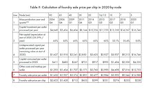
TSMC, one of the biggest silicon manufacturers in the world, usually doesn't disclose company pricing of the silicon it manufactures and only shares that with its customers. It appears that RetiredEngineer (@chiakokhua on Twitter) got a hold of the pricing of TSMCs wafers on every manufacturing node starting from 90 nm down to 5 nm. That includes a wide portfolio of 65, 40, 28, 20, 16/12, 10, and 7 nm nodes as well. The table shown below includes information dating to April 2020, so it is possible that some things are now different and they surely are. There are a few quite interesting notes from the image, namely the price increase as the node shrinks.

From 90 nm to 20 nm, the price of the wafer didn't increase as much, however, starting from 16/12 nm node(s), TSMC has seen costs per wafer, and other costs increase exponentially. For example, just compare the 10 nm wafer price of $5992 with the price of a 5 nm wafer which costs an amazing $16988. This is more than a 180% price increase in just three years, however, the cost per transistor is down as you get around 229% higher density in that period, making TSMC actually in line with Moore's Law. That is comparing Transistor density (MTr / mm²) of52.51 million transistors for the 10 nm node and 173 million transistors per mm² of the 5 nm node .

Rambus Advances HBM2E Performance to 4.0 Gbps for AI/ML Training Applications

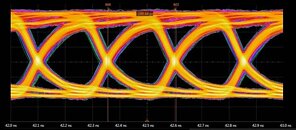
Rambus Inc. (NASDAQ: RMBS), a premier silicon IP and chip provider making data faster and safer, today announced it has achieved a record 4 Gbps performance with the Rambus HBM2E memory interface solution consisting of a fully-integrated PHY and controller. Paired with the industry's fastest HBM2E DRAM from SK hynix operating at 3.6 Gbps, the solution can deliver 460 GB/s of bandwidth from a single HBM2E device. This performance meets the terabyte-scale bandwidth needs of accelerators targeting the most demanding AI/ML training and high-performance computing (HPC) applications.

"With this achievement by Rambus, designers of AI and HPC systems can now implement systems using the world's fastest HBM2E DRAM running at 3.6 Gbps from SK hynix," said Uksong Kang, vice president of product planning at SK hynix. "In July, we announced full-scale mass-production of HBM2E for state-of-the-art computing applications demanding the highest bandwidth available."

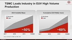
TSMC Owns 50% of All EUV Machines and Has 60% of All EUV Wafer Capacity

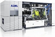
TSMC had been working super hard in the past few years and has been investing in lots of new technologies to drive the innovation forward. At TSMC's Technology Symposium held this week was, the company has presented various things like the update on its 12 nm node, as well as future plans for node development. One of the most interesting announcements made this week was TSMC's state and ownership of Extreme Ultra-Violet (EUV) machines. ASML, the maker of these EUV machines used to etch the pattern on silicon, has been the supplier of the Taiwanese company. TSMC has announced that they own an amazing 50% of all EUV machine installations.

What is more important is the capacity that the company achieves with it. It is reported that TSMC achieves 60% of all EUV wafer capacity in the world, which is a massive achievement of what TSMC can do with the equipment. The company right now has only two nodes on EUV in high-volume manufacturing, the 7 nm+ node and 5 nm node (which is going HVM in Q4), however, that is more than any of its competitors. All of the future nodes are to be manufactured using the EUV machines and the smaller nodes require it. As far as the competitors go, only Samsung is currently making EUV silicon on the 7 nm LPP node. Intel is yet to release some products on a 7 nm node of its own, which is the first EUV node from the company.

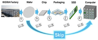
Kioxia Plans for Wafer-Level SSD

Wafer-scale design is getting popular it seems. Starting from the wafer-scale engine presented by Cerebras last year, which caused quite the shakeup in the industry, it seems that this design approach might be more useful than anyone thought. During VLSI Symposium 2020, Shigeo Oshima, Chief Engineer at Kioxia, had a presentation about new developments in SSD designs and implementations. What was one of the highlights of the presentation was the information that Kioxia is working on, was a technology Kioxia is referring to as wafer-level SSD.

The NAND chips used in SSDs would no longer be cut from the wafer and packaged separately. Instead, the wafer itself would represent the SSD. This is a similar approach Cerebras used with its wafer-scale engine AI processor. What would be gains of this approach compared to traditional methods of cutting up NAND chips and packaging them separately you might wonder? Well, for starters you wouldn't need to cut the wafer, package individual memory chips, and build the SSD out of them. Those steps could be skipped and there would be some cost savings present. And imagine if you decide to do wafer stacking. You could build super scaling SSDs with immense performance capable of millions of IOPS. However, for now, this is only a concept and it is just in early development. There is no possibility to find it in a final product anytime soon.
Kioxia Wafer-Level SSD
Return to Keyword Browsing
May 15th, 2024 14:28 EDT change timezone

New Forum Posts

Popular Reviews

Controversial News Posts