News Posts matching #Xe

Return to Keyword Browsing

TSMC Allocation the Next Battleground for Intel, AMD, and Possibly NVIDIA

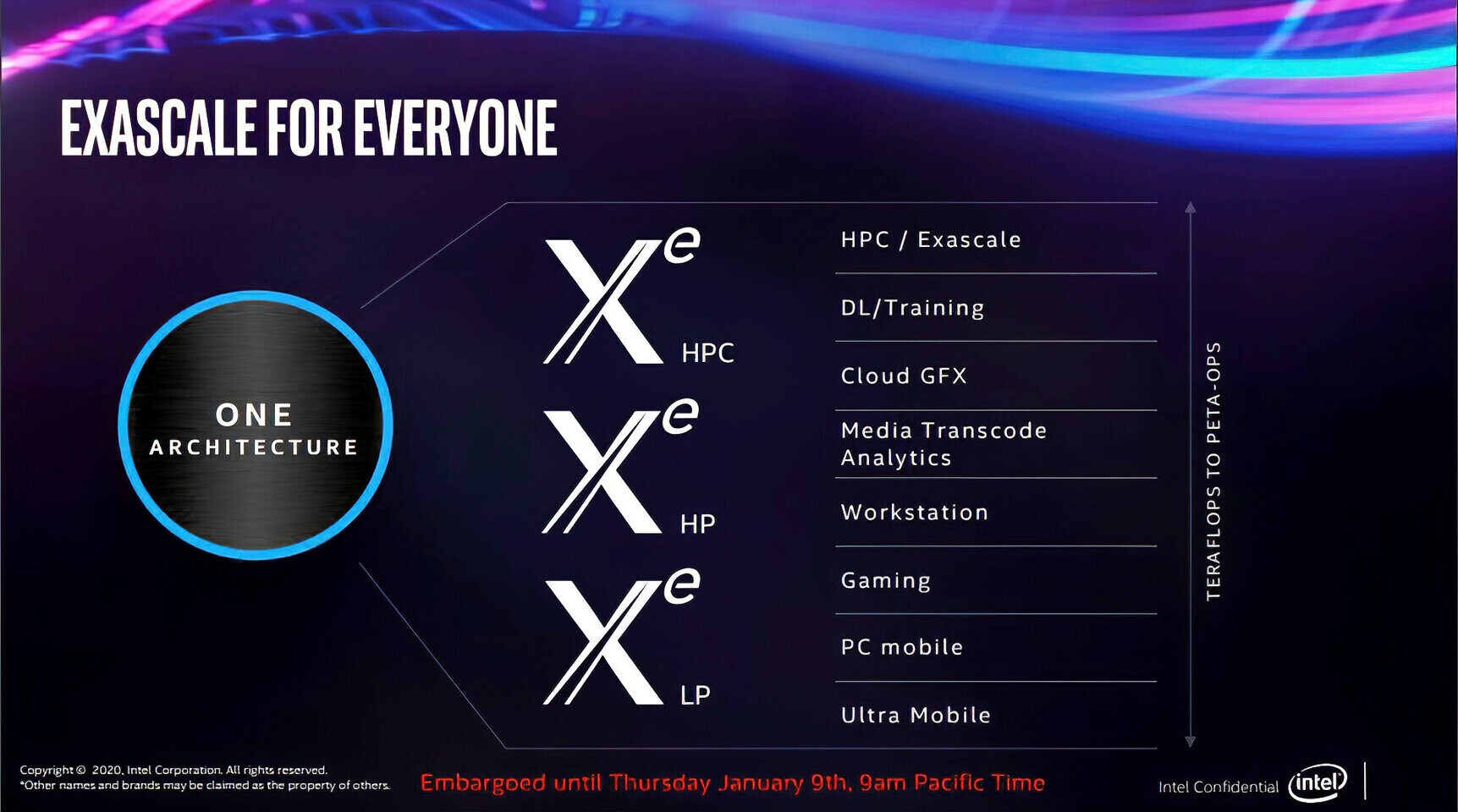
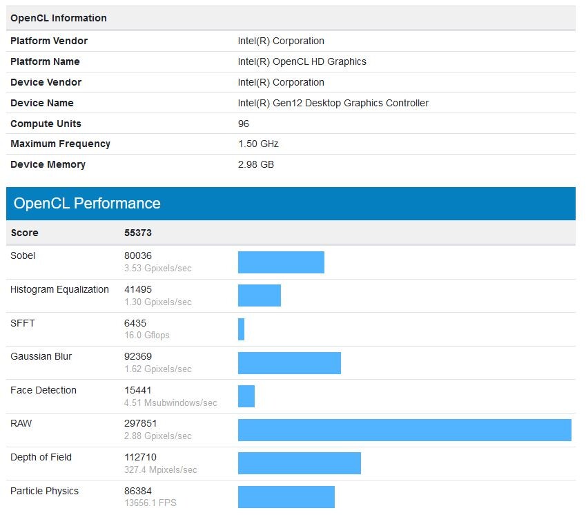
With its own 7 nm-class silicon fabrication node nowhere in sight for its processors, at least not until 2022-23, Intel is seeking out third-party semiconductor foundries to support its ambitious discrete GPU and scalar compute processor lineup under the Xe brand. A Taiwanese newspaper article interpreted by Chiakokhua provides a fascinating insight to the the new precious resource in the high-technology industry - allocation.

TSMC is one of these foundries, and will give Intel access to a refined 7 nm-class node, either the N7P or N7+, for some of its Xe scalar compute processors. The company could also seek out nodelets such as the N6. Trouble is, Intel will be locking horns with the likes of AMD for precious foundry allocation. NVIDIA too has secured a certain allocation of TSMC 7 nm for some of its upcoming "Ampere" GPUs. Sources tell China Times that TSMC will commence mass-production of Intel silicon as early as 2021, on either N7P, N7+, or N6. Business from Intel is timely for TSMC as it is losing orders from HiSilicon (Huawei) in wake of the prevailing geopolitical climate.

Intel to Detail Xe Graphics on August 13

Intel is expected to reveal technical details of its upcoming Xe graphics architecture on August 13, according to a tweet by Intel Graphics that has since been deleted. Tom's Hardware believes the reveal is still on the cards. "You've waited. You've wondered. We'll deliver. In 20 days, expect more details on Xe graphics," the tweet read. Senior Fellow and Director of Graphics Architecture at Intel, David Blythe is expected to present a technical brief on the Xe graphics architecture at a Hot Chips 2020 virtual event on August 17.

These technical reveals are closely timed with the launch of "Tiger Lake," Intel's first commercial debut of Xe as an iGPU solution the chipmaker refers to as "Gen12" for consistency with older generations of integrated graphics. Xe is far from designed for just iGPU or small dGPUs, with the architecture being scalable all the way up to large scalar compute processors the size of beer mug coasters. Even as an iGPU, Xe is formidable, as it was recently shown playing AAA games by itself. Recent commentary from Intel at its Q2 2020 financial results provided strong hints of Xe dGPUs being de-coupled from Intel's foundry woes, and possibly headed for third-party foundries such as Samsung or TSMC.

Intel 7nm CPUs Delayed by a Year, Alder Lake in 2H-2021, Other Commentary from Intel Management

Intel's silicon fabrication woes refuse to torment the company's product roadmaps, with the company disclosing in its Q2-2020 financial results release that the company's first CPUs built on the 7 nanometer silicon fabrication node are delayed by a year due to a further 6-month delay from prior expectations. The company will focus on getting its 10 nm node up to scale in the meantime.

The company mentioned that the 10 nm "Tiger Lake" mobile processor and "Ice Lake-SP" enterprise processor remains on-track for 2020. The company's 12th Generation Core "Alder Lake-S" desktop processors won't arrive before the second half of 2021. In the meantime, Intel will launch its 11th Gen Core "Rocket Lake" processor on the 14 nm node, but with increased IPC from the new "Cypress Cove" CPU cores. Also in 2H-2021, the company will launch its "Sapphire Rapids" enterprise processors that come with next-gen connectivity and updated CPU cores.
Intel 7 nanometer delay

MSI References 11th Gen "Rocket Lake" in its H410-based Prebuilt Manual

In a clear sign of Intel's 11th Gen Core "Rocket Lake-S" desktop processors being prepared to support the company's 400-series chipsets, including the entry-level H410, the Russian language manual of the company's Infinite 915 pre-built compact gaming desktop that uses an Intel H410 chipset motherboard. The manual references support for the 65 W TDP versions of "CML-S" (10th Gen "Comet Lake-S") and "RKL-S" (11th Gen "Rocket Lake-S") processors in the manual. Besides increased IPC (single-threaded performance) riding on the new "Cypress Cove" CPU cores that are a backport of "Willow Cove" to the 14 nm process, "Rocket Lake-S" features an updated Gen12 Xe iGPU.

Intel Linux Patch Confirms "Alder Lake" is a Hybrid Core Processor

A Linux kernel patch contributed and signed off by Intel confirms that its upcoming Core "Alder Lake" processor will feature a hybrid core topology, much like Core Hybrid "Lakefield." The patch references "Lakefield" and "Alder Lake" under "Hybrid Core/Atom Processors." The patch possibly gives the Linux kernel awareness of the hybrid core topology, so it can schedule its work between the two types of cores on the silicon accordingly, and avoid rotating between the two core groups. Under the Android project, Linux has been aware of a similar tech from Arm since 2013.

Analogous with Arm big.LITTLE, the Intel Hybrid Core technology involves two kinds of CPU cores on a processor die, the first kind being "high performance," and the second being "low power." On "Lakefield," Intel deployed one "Sunny Cove" high performance core, and four "Tremont" low power cores. The low power cores keep the machine ticking through the vast majority of time when processing workloads requiring the high performance cores aren't present. With "Alder Lake," Intel is expected to scale up this concept, with the silicon rumored to feature eight "Golden Cove" high performance cores, and eight "Gracemont" low power ones. The chip is also expected to feature a Gen12 Xe iGPU.

Intel Apparently Reusing Iris Branding for Xe Integrated Graphics; Tiger Lake With 768 Shading Units Spotted

Another day, another Intel Tiger Lake and Xe graphics leak. This time, it comes courtesy of secret benchmark spotter extraordinaire TUM_APISAK, who spotted an Intel Tiger Lake CPU with integrated graphics on SiSoftware. Tiger Lake will ship with a graphics capability that reaches at least 96 Execution units (which boils down to the referred 768 Shading Units), which corresponds to the graphics prowess available on Intel's (currently discrete) DG1-SDV. The Iris Xe graphics on this benchmark are running at 1.3 GHz, with a 6.3 GB of memory on their elbow.

Intel Gen12 iGPU on "Rocket Lake" will be Slimmer than the one on "Tiger Lake"?

The Gen12 Xe integrated graphics component of the upcoming "Rocket Lake-S" desktop processor will be slimmer than the one on the upcoming 10 nm "Tiger Lake" silicon, according to a Geekbench hardware detection unearthed by TUM_APISAK. An 8-core/16-thread "Rocket Lake-S" sample surfaced on the Geekbench database, which shows the iGPU to feature 32 compute units as read by the OpenCL benchmark (corresponding with 32 execution units), compared to 96 on the "Tiger Lake-U" mobile processor die. The iGPU is also clocked rather conservatively on this ES, at at 1.15 GHz. The CPU component, on the other hand, ticks at 3.20 GHz, boosting up to 4.30 GHz. It's likely that with the power budget of the desktop platform, the iGPU will be able to sustain boost frequencies better.

Acer Announces Swift 5 Notebooks Powered by Intel "Tiger Lake" Processors

Acer today announced its new Swift 5 notebook that offers a new take on productivity, powerful yet light enough to be carried around throughout the day. The ultraportable device is a beacon of both design and performance, sporting a professional aesthetic that is backed up by impressive functionality. This year's model features ultra-narrow bezels that allow for a 90% screen-to-body ratio, a touchscreen with Antimicrobial Corning Gorilla Glass and new colors, such as mist green.

"The new Swift 5 pushes the envelope on what thin-and-light notebooks can be," said James Lin, General Manager, Notebooks, IT Products Business, Acer Inc. "A productivity powerhouse housed in a sleek and ultraportable chassis, the Swift 5 is an excellent option for professionals who are always on the move and seeking a device capable of keeping up with them."

Intel "Tiger Lake" Gen12 Xe iGPU Shown Playing "Battlefield V" By Itself

In what is possibly the first taste of Intel's Gen12 Xe iGPU running a AAA game, Ryan Shrout, chief performance strategist at Intel, showed off a prototype notebook running a "Tiger Lake" processor that is playing "Battlefield V" by itself (without discrete graphics). "Perks of the job! Took a prototype Tiger Lake system for a spin on Battlefield V to stretch its legs. Impressive thin and light gaming perf with Xe graphics! Early drivers/sw, but it's the first time I've seen this game run like this on integrated gfx. More later this year!," said Shrout.

The gameplay video (linked as source below), shows a playable experience for "Battlefield V" with Gen12 Xe, with 1080p at around 30 Hz. It only serves to appetize us for what would come next, when Intel scales up this IP to discrete GPUs. The Gen12 Xe iGPU appears capable of e-sports gaming with the right settings, and could spell serious trouble for cheap dGPU solutions such as the GeForce MX series or Radeon RX 530 series.

Intel "Rocket Lake-S" a Multi-Chip Module of 14nm Core and 10nm Uncore Dies?

VLSI engineer and industry analyst, @chiakokhua, who goes by "Retired Engineer" on Twitter, was among the very first voices that spoke about 3rd gen Ryzen socket AM4 processors being multi-chip modules of core- and uncore dies built on different silicon fabrication processes, which was an unbelievable theory at the time. He now has a fantastic theory of what "Rocket Lake-S" could look like, dating back to November 2019, which is now re-surfacing on tech communities. Apparently, Intel is designing these socket LGA1200 processors to be multi-chip modules, similar to "Matisse" in some ways, but different in others.

Apparently, "Rocket Lake-S" is a multi-chip module of a 14 nm die that holds the CPU cores; and 10 nm die that holds the uncore components. AMD "Matisse" and "Vermeer" too have such a division of labor, but the CPU cores are located on dies with a more advanced silicon fabrication process (7 nm), than the die with the uncore components (12 nm).

Intel "Tiger Lake" Gen12 Xe iGPU Compared with AMD "Renoir" Vega 8 in 3DMark "Night Raid"

Last week, reports of Intel's Gen12 Xe integrated graphics solution catching up with AMD's Radeon Vega 8 iGPU found in its latest Ryzen 4000U processors in higher-tier 3DMark tests sparked quite some intrigue. AMD's higher CPU core-count bailed the processor out in overall 3DMark 11 scores. Thanks to Thai PC enthusiast TUM_APISAK, we now have a face-off between the Core i7-1165G7 "Tiger Lake-U" processor (15 W), against AMD Ryzen 7 4800U (15 W), and the mainstream-segment Ryzen 7 4800HS (35 W), in 3DMark "Night Raid."

The "Night Raid" test is designed to evaluate iGPU performance, and takes advantage of DirectX 12. The Core i7-1165G7 falls behind both the Ryzen 7 4800U and the 4800HS in CPU score, owing to its lower CPU core count, despite higher IPC. The i7-1165G7 is a 4-core/8-thread chip featuring "Willow Cove" CPU cores, facing off against 8-core/16-thread "Zen 2" CPU setups on the two Ryzens. Things get interesting with graphics tests, where the Radeon Vega 8 solution aboard the 4800U scores 64.63 FPS in GT1, and 89.41 FPS in GT2; compared to just 27.79 FPS in GT1 and 32.05 FPS in GT2, by the Gen12 Xe iGPU in the i7-1165G7.

Intel "Tiger Lake" Beats AMD "Renoir" in Graphics Tests under 3D Mark

Now, take that title with the customary grain of salt, and remember: most mobile configurations aren't directly comparable due to different components, speed of the memory subsystem, and so on. Putting that salt aside, though, one thing remains: Intel beats AMD in the latest purported 3DMark benchmarks - and on the red team's home-field, so to speak: graphics performance. A benchmark posted by renowned leaker and benchmark scavenger rogame on twitter has turned up an Intel Tiger Lake-U (i7-1165G7) scoring 11879 (99.68%) in the Physics and 6912 (112.92%) in the Graphics score compared to AMD's R7 4800U 11917 Physics score and 6121 Graphics score.

For context, this pits a 4-core, 8-thread Intel Willow Cove design paired with Gen12 Xe graphics tech (2.8 GHz base, 4.4 GHz boost) against 8 of AMD's Zen 2 cores and Vega graphics. Also for context, it's expected that Intel's i7-1165G7 runs with a 28 W TDP, compared to AMD's R7 4800U 15 W envelope. Also of note is that 3D Mark isn't exactly the poster-child for CPU parallelization performance, as the benchmark scales up rather poorly as more cores are added. Perhaps more interesting as a comparison, these scores from Intel's Tiger Lake are comparable to the company's current i5-10300H (4C/8T 2.5 GHz base 4.5 GHz boost), which scores 10817 on the Physics side (making the i7-1165G7 9.8% faster with a 200 MHz slower base clock, 100 MHz higher boost & 17 W less TDP (28 W for the Tier Lake and 45 W for the i5-10300H).

Intel "Tiger Lake" vs. AMD "Renoir" a Pitched Battle on 3DMark Database

Intel's 11th generation Core i7-1165G7 "Tiger Lake-U" processor armed with 4 "Willow Cove" cores and Gen12 Xe graphics fights a pitched battle against AMD Ryzen 7 4800U "Renoir" (8 "Zen 2" cores and Radeon Vega 8 graphics), courtesy of some digging by Thai PC enthusiast TUM_APISAK. The 4800U beats the i7-1165G7 by a wafer-thin margin of 1.9% despite double the CPU core-count and a supposedly advanced iGPU, with 6331 points as against 6211 points of the Intel chip, in 3DMark 11. A breakdown of the score reveals fascinating details of the battle.

The Core i7-1165G7 beats the Ryzen 7 4800U in graphics tests, with a graphics score of 6218 points, against 6104 points of the 4800U, resulting in a 1.9% lead. In graphics tests 1, 2, and 3, the Gen12 Xe iGPU is 7.3-8.9% faster than the Radeon Vega 8, through translating to 2-4 FPS. The Intel iGPU crosses the 30 FPS mark in these three tests. With graphics test 4, the AMD iGPU ends up 8.8% faster. Much of AMD's performance gains come from its massive 55.6% physics score lead thanks to its 8-core/16-thread CPU, which ends up beating the 4-core/8-thread "Willow Cove," with the 4800U scoring 12494 points compared to 8028 points for the i7-1165G7. This CPU muscle also plays a big role in graphics test 4. This battle provides sufficient basis to speculate that "Tiger Lake-U" will have a very uphill task matching "Renoir-U" chips such as the Ryzen 7 4800U, and the upcoming Ryzen 9 4900U (designed to compete with the i7-1185G7).

No Intel "Rocket Lake-S" or "Ice Lake-X" This Year?

A roadmap slide from an Intel Partner Connect presentation suggests that the company's client-segment processor lineup will be unchanged for the rest of 2020, with the company briskly launching its 10th generation "Comet Lake-S" desktop processor lineup through May-June, and "Comet Lake-H" a month prior. The Core X "Cascade Lake-X" processor lineup will continue to lead the company in the high core-count HEDT segment, with no indications of new models, at least none higher than 18 cores.

More importantly, this slide dulls expectations of the company refreshing its desktop process segment just before Holiday 2020 with the 11th generation "Rocket Lake-S" silicon that has next-gen "Willow Cove" CPU cores, Gen12 Xe integrated graphics, and PCIe gen 4.0 connectivity, especially with engineering samples of the chips already hitting the radar. Intel is expected to launch 10 nm "Ice Lake-SP" Xeon enterprise processors in 2020, and there was hope for some of this IP to power Intel's next HEDT platform, the fabled "Ice Lake-X," especially with AMD's "Castle Peak" 3rd gen Threadrippers dominating this segment. While there's little doubt that the slide may have originated from Intel, its context must be studied. Partner Connect is a platform for Intel to interact with its channel partners (distributors, retailers, system integrators, etc), and information about future products is far more restricted on these slides, than presentations intended for large OEMs, motherboard manufacturers, etc. Then again, with the COVID-19 pandemic throwing supply chains off rails, it wouldn't surprise us if this slide spells Gospel.

Intel 8-core/16-thread "Rocket Lake-S" Processor Engineering Sample 3DMarked

The "Rocket Lake-S" microarchitecture by Intel sees the company back-port its next-generation "Willow Cove" CPU core to the existing 14 nm++ silicon fabrication process in the form of an 8-core die with a Gen12 Xe iGPU. An engineering sample of one such processor made it to the Futuremark database. Clocked at 3.20 GHz with 4.30 GHz boost frequency, the "Rocket Lake-S" ES was put through 3DMark "Fire Strike" and "Time Spy," with its iGPU in play, instead of a discrete graphics card.

In "Fire Strike," the "Rocket Lake-S" ES scores 18898 points in the physics test, 1895 points in the graphics tests, and an overall score of 1746 points. With "Time Spy," the overall score is 605, with a CPU score of 4963 points, and graphics score of 524. The 11th generation Core "Rocket Lake-S" processor is expected to be compatible with existing Intel 400-series chipset motherboards, and feature a PCI-Express gen 4.0 root complex. Several 400-series chipset motherboards have PCIe gen 4.0 preparation for exactly this. The increased IPC from the "Willow Cove" cores is expected to make the 8-core "Rocket Lake-S" a powerful option for gaming and productivity tasks that don't scale across too many cores.

Intel Scores Another AMD Graphics Higher-up: Ali Ibrahim

To support its efforts to build a competitive consumer GPU lineup under the Xe brand, which Intel likes to call its "Odyssey," the company scored another higher-up from AMD, this time Ali Ibrahim. He joined Intel this month as a vice-president within the Architecture, Graphics and Software group, although the company didn't specify his responsibilities. "We are thrilled that Ali has joined Intel as Vice President, Platform Architecture and Engineering - dGPUs to be part of the exciting Intel Xe graphics journey," said an Intel spokesperson in a comment to CRN.

During his 13-year tenure at AMD, Ali Ibrahim was the chief-architect of the company's cloud gaming and console SoC businesses, which provides valuable insight into Intel's breakneck efforts to build high-end discrete GPUs (something it lacked for the past two decades). Intel is the only other company that is capable of building semi-custom chips for someone like Microsoft or Sony as the inventor of x86, provided it has a GPU that can match AMD's in the console space. Likewise, with gaming taking baby steps to the cloud as big players such as Google betting on it, Intel sees an opportunity for cloud gaming GPUs that aren't too different from its "Ponte Vecchio" scalar processors. The transfer of talent isn't one-way, as AMD recently bagged Intel's server processor lead Dan McNamara to head the EPYC brand.

New Details Surface on Intel NUC 11 Extreme: TigerLake-U & GTX 1660 Ti

New details have surfaced on Intel's next-generation NUC systems - built with the intention to carry the highest performance density per available chassis capacity in the computer market (the aim is a 1.35 L case). We already knew Intel's Panther Canyon NUC would bring about their Tiger Lake-U designs would be carrying the company's Tiger Lake-U CPUs, which should combine next-generation "Willow Cove" CPU cores with an iGPU based on Intel's new Xe graphics architecture. A new piece of data here, as has been reported, is that Intel is also working on an enthusiast-class NUC under the "Phantom Canyon" moniker, which should bring about increased graphics performance.

Even if Intel's graphics architecture is a mindblowing performance improvement over their current graphics technologies, there's only so much an integrated graphics solution can do. Now, we seemingly have confirmation, via a 3D Max Benchmark, that Intel's Panther Canyon will be paired with an NVIDIA GeForce 1660 Ti graphics card (scoring 5,355 points). The 3D Mark TimeSpy test system uses a TigerLake-U engineering sample clocked at 2.3 GHz base and 4.4 GHz boost, alongside an 80 W NVIDIA GTX 1660 Ti (Notebook) and 8 GB of RAM.

Intel Rocket Lake CPU Appears with 6 Cores and 12 Threads

We have been hearing a lot about Intel's Rocket Lake lineup of processors. They are supposed to be a backport of Willow Cove 10 nm core, adapted to work on a 14 nm process for better yielding. Meant to launch sometime around late 2020 or the beginning of 2021, Rocket Lake is designed to work on the now existing LGA1200 socket motherboards, which were launched just a few days ago along with Intel Comet Lake CPUs. Rocket Lake is there to supply the desktop segment and satisfy user demand, in light of lacking 10 nm offers for desktop users. The 10 nm node is going to present only on mobile/laptop and server solutions before it comes to the desktop.

In the latest report on 3D Mark, the hardware leaker TUM APISAK has found a Rocket Lake CPU running the benchmark and we get to see first specifications of the Rocket Lake-S platform. The benchmark ran on 6 core model with 12 threads, that had a base clock of 3,5 GHz. The CPU managed to boost up to 4,09 GHz, however, we are sure that these are not final clocks and the actual product should have even higher frequencies. Paired with Gen12 Xe graphics, the Rocket Lake platform could offer a very nice alternative to AMD offerings if the backport of Willow Cove goes well. Even though it is still using a 14 nm node, performance would be good. The only things that would be sacrificed (from backporting) are die space and efficiency/heat.
Intel Rocket Lake Benchmark Report

Intel Gen12 Xe iGPU Twice as Fast as Gen11, Enters AMD Vega iGPU Territory

Intel Xe graphics architecture makes its commercial debut as an iGPU solution in the company's upcoming "Tiger Lake" mobile processors. The iGPU can be configured along three tiers, with GT1 featuring 48 execution units (EUs), GT2 80 EUs, and GT3 leading the pack with 96 EUs, all within a 15 W envelope (for the total chip). There's a higher tier still of GT3 that comes with higher boost frequencies, tapping into the chip's overall increased 28 W TDP, but this variant of "Tiger Lake" could likely be an Apple-exclusive like its "Ice Lake" based predecessor.

NotebookCheck compiled a 3DMark FireStrike comparison between the various tiers of the Xe iGPU, and compared it to the Gen11 iGPU found with current-generation "Ice Lake-U" processors. The graph doesn't put out scores, but relative performance. Apparently, the 48 EU version of Gen12 Xe is a little over twice as fast as Gen11 GT1, and faster than even the 64 EU Gen11 GT2. The Gen12 GT2 with 80 EUs is around 1.7x faster than the Gen11 GT2 (64 EU). The 96 EU GT3 trim is over twice as fast, and its 28 W variant faster still. These performance give Gen12 a shot against AMD's Radeon Vega-based iGPU solution found in "Renoir." AMD has slimmed the number of CUs down to 8 (512 SP) with "Renoir," down from 11 CUs in the previous generation, compensating for it with higher GPU engine clocks.

Intel Gen12 Xe DG1 OpenCL Performance Geekbenched

Intel's ambitious Xe graphics architecture is expected to make its first commercial debut as an iGPU that's part of the company's 11th gen Core "Tiger Lake" mobile processors, but it already received a non-commercial distribution as a discrete GPU called the DG1, with Intel shipping it to its independent software vendor ecosystem partners to begin exploratory work on Xe. One such ISV paired the card with a Core i7-8700 processor, and put it through Geekbench. While the Geekbench device identification doesn't mention "DG1," we lean toward the possibility looking at its 96 EU configuration, and 1.50 GHz clock speed, and 3 GB memory.

The Geekbench run only covers OpenCL performance of the selected device: "Intel(R) Gen12 Desktop Graphics Controller." The total score is 55373 points, with 3.53 Gpixels/s in "Sorbel," 1.30 Gpixels/sec in Histogram Equalization, 16 GFLOPs in SFFT, 1.62 GPixels/s in Gaussian Blur, 4.51 Msubwindows/s in Face Detection, 2.88 Gpixels/s in RAW, 327.4 Mpixels/s in DoF, and 13656 FPS in Particle Physics. These scores roughly match the 11 CU Radeon Vega iGPU found in AMD "Picasso" Ryzen 5 3400G processors.

Intel "Tiger Lake-U" Processor with Relatively High Clock Speed Spotted

An unnamed Intel "Tiger Lake-U" quad-core processor was spotted on Futuremark database by _rogame, featuring 2.80 GHz nominal clock-speeds. Barring the 28 W i7-1068NG7 and i5-1038NG7, which are exclusive for MacBooks and aren't considered U-segment, all current-gen "Ice Lake" client chips have their nominal clock speeds ranging between 1.00 to 1.30 GHz. Given this, 2.80 GHz would qualify as a big jump for a U-segment "Tiger Lake" chip. We know from a separate report that "Tiger Lake" could also offer Turbo Boost frequencies as high as 4.70 GHz for the top Core i7-1185G7 part, a similar jump from the 3.90 GHz max boost of the current-gen i7-1065G7, all while retaining a 15 W nameplate TDP.

The Futuremark database listing only mentions nominal clock of 2.80 GHz, and the CPU core configuration of 4-core/8-thread. The hardcoded CPU name string of this prototype specifies "Tiger Lake U," confirming this is a 15 W part, and not a 28 W part that will be gobbled down by Apple. Intel's newfound clock-speed headroom could be attributed to the company's refined 10 nm+ silicon fabrication node. "Tiger Lake" combines "Willow Cove" CPU cores with an iGPU based on the company's ambitious new Xe graphics architecture, marking its commercial debut. "Tiger Lake" is expected to launch around September-October, 2020.

Hot Chips 2020 Program Announced

Today the Hot Chips program committee officially announced the August conference line-up, posted to hotchips.org. For this first-ever live-streamed Hot Chips Symposium, the program is better than ever!

In a session on deep learning training for data centers, we have a mix of talks from the internet giant Google showcasing their TPUv2 and TPUv3, and a talk from startup Cerebras on their 2nd gen wafer-scale AI solution, as well as ETH Zurich's 4096-core RISC-V based AI chip. And in deep learning inference, we have talks from several of China's biggest AI infrastructure companies: Baidu, Alibaba, and SenseTime. We also have some new startups that will showcase their interesting solutions—LightMatter talking about its optical computing solution, and TensTorrent giving a first-look at its new architecture for AI.
Hot Chips

NVIDIA Ampere A100 Has 54 Billion Transistors, World's Largest 7nm Chip

Not long ago, Intel's Raja Koduri claimed that the Xe HP "Ponte Vecchio" silicon was the "big daddy" of Xe GPUs, and the "largest chip co-developed in India," larger than the 35 billion-transistor Xilinix VU19P FPGA co-developed in the country. It turns out that NVIDIA is in the mood for setting records. The "Ampere" A100 silicon has 54 billion transistors crammed into a single 7 nm die (not counting transistor counts of the HBM2E memory stacks).

NVIDIA claims a 20 Times boost in both AI inference and single-precision (FP32) performance over its "Volta" based predecessor, the Tesla V100. The chip also offers a 2.5X gain in FP64 performance over "Volta." NVIDIA has also invented a new number format for AI compute, called TF32 (tensor float 32). TF32 uses 10-bit mantissa of FP16, and the 8-bit exponent of FP32, resulting in a new, efficient format. NVIDIA attributes its 20x performance gains over "Volta" to this. The 3rd generation tensor core introduced with Ampere supports FP64 natively. Another key design focus for NVIDIA is to leverage the "sparsity" phenomenon in neural nets, to reduce their size, and improve performance.

TSMC 5 nm Customers Listed, Intel Rumored to be One of Them

TSMC is working hard to bring a new 5 nm (N5 and N5+) despite all the hiccups the company may have had due to the COVID-19 pandemic happening. However, it seems like nothing can stop TSMC, and plenty of companies have already reserved some capacity for their chips. With mass production supposed to start in Q3 of this year, 5 nm node should become one of the major nodes over time for TSMC, with predictions that it will account for 10% of all capacity for 2020. Thanks to the report of ChinaTimes, we have a list of new clients for the TSMC 5 nm node, with some very interesting names like Intel appearing on the list.

Apple and Huawei/HiSilicon will be the biggest customers for the node this year with A14 and Kirin 1000 chips being made for N5 node, with Apple ordering the A15 chips and Huawei readying the Kirin 1100 5G chip for the next generation N5+. From there, AMD will join the 5 nm party for Zen 4 processors and RDNA 3 graphics cards. NVIDIA has also reserved some capacity for its Hopper architecture, which is expected to be a consumer-oriented option, unlike Ampere. And perhaps the most interesting entry to the list is Intel Xe graphics cards. The list shows that Intel might use the N5 process form TSMC so it can ensure the best possible performance for its future cards, in case it has some issues manufacturing its own nodes, just like it did with 10 nm.
TSMC 5 nm customers

Intel Gen12 Xe GPU with 96 Execution Units Shows Up on SiSoft Database

An Intel Gen12 Xe GPU, possibly a discrete- DG1 prototype, showed up on the SiSoft SANDRA online database. The GPU is detailed by SANDRA as having 768 unified shaders across 96 execution units (EUs), a 1.50 GHz GPU clock speed, 1 MB of on-die L2 cache, and 3 GB of dedicated video memory of an unknown type (likely GDDR6). This is probably a different chip from the DG1-SDV, which caps out at 900 MHz GPU clock, although its SIMD muscle is identical.

At a clock-speed of 1.50 GHz, the chip would feature an FP32 throughput of 2,303 GFLOPs (we know this from the DG1-SDV offering 1382 GFLOPs at 900 MHz). If the software-side optimization backs this hardware, the resulting product could end up with performance in the league of the 8 CU Radeon "Vega" solution found in the AMD "Renoir" APU, or the Radeon RX 560 discrete GPU, which are just about enough for PUBG at 1080p with medium settings.
Return to Keyword Browsing
May 21st, 2024 13:27 EDT change timezone

New Forum Posts

Popular Reviews

Controversial News Posts