News Posts matching #Zen 3

Return to Keyword Browsing

AMD Ryzen 4000 Series "Vermeer" CPUs to be Compatible with B450 Motherboards

AMD's upcoming Ryzen 4000 series "Vermeer" lineup of CPUs based on the new Zen 3 core is slated to launch sometime in late 2020, and we have information about the chipset support of 4th generation of Ryzen CPUs. The laptop manufacturer XMG, known for its crazy Apex 15 laptop with 16 core AMD Ryzen 3950X CPU inside, has posted a Reddit thread about its new laptop. In the thread, XMG has listed specifications of the laptop, and in one point it mentions support for Ryzen 4000 series of CPUs. XMG has written that the B450 motherboards will be supporting the next generation CPUs simply by microcode updates AMD will push to OEMs. XMG uses the B450 chipset in its laptops, so they are presumably going to offer some configurations with Ryzen 4000 CPUs in the future. This information is good news for everybody who has a motherboard with a B450 chipset as they can get a bit more mileage out of it.
XMG Apex 15 Specifications

AMD 4th Gen Ryzen Desktop Processors to Launch Around September 2020

AMD's 4th generation Ryzen desktop processors are expected to launch around September 2020, sources in the motherboard industry tell DigiTimes. Codenamed "Vermeer," successor to "Matisse," these processors will be socket AM4 multi-chip modules of up to two CPU complex dies based on the "Zen 3" microarchitecture, combined with an I/O controller die. The "Zen 3" chiplets are expected to be fabricated on a newer 7 nm-class process by TSMC, either N7P or N7+. The biggest design change with "Zen 3" is the doing away of CCX arrangement of CPU cores, with each chiplet holding a common block of cores sharing a last-level cache. This, along with clock speed headroom gains from the new node are expected to yield generational price-performance increases.

The "Zen 2" based 8-core "Renoir" die is also expected to make its socket AM4 debut within 2020, succeeding the "Picasso" based quad-core Ryzen 3000-series APUs. This is a particularly important product for AMD, as it is expected to compete with Intel's 10th generation Core i5 6-core/12-thread processors in terms of pricing, while offering more cores (8-core/16-thread) and a faster iGPU. The 4th gen Ryzen socket AM4 processor lineup will launch alongside AMD's 600-series motherboard chipset, with forwards- and backwards-compatibility (i.e., "Vermeer" and "Renoir" working with older chipsets, and older AM4 processors working on 600-series chipset motherboards). AMD was originally expected to unveil these processors at the 2020 Computex trade-show in June, but Computex itself is rescheduled to late-September.

AMD Ryzen 4000 Rumored to Bring 15% IPC Uplift

AMD's Zen 3 architecture will power the next generation Ryzen 4000 desktop chips and the 3rd Gen EPYC lineup which are both expected to launch later this year. Adored TV has received some leaked information detailing the technical specifications of the Zen 3 architecture. The majority of the leaked information confirmed existing rumors such as the 8 core CCX, higher clocks and lower power draw.

However the leak suggests IPC improvements will be less than the expected 20% hinted at by AMD and may end up being closer to 10 - 15%. The leak also claims that L3 cache will remain at 32 MB however it will no longer be split due to the single CCX. While this may be disappointing for some, remember to take the claims with a grain of salt as with any rumor.
Leak

AMD Sheds Light on the Missing "+" in "7nm" for Zen 3 and RDNA2 in its Latest Presentation

AMD at its Financial Analyst Day 2020 presentation made a major clarification about its silicon fabrication process. It was previously believed that the company's upcoming "Zen 3" CPU microarchitecture and RDNA2 graphics architectures were based on TSMC's N7+ (7 nm EUV) silicon fabrication process because AMD would mark the two as "7 nm+" in its marketing slides. Throughout its Financial Analyst Day presentation, however, AMD avoided using that marker, and resorted to an amorphous "7 nm" marker, prompting one of the financial analysts to seek a clarification. At the time, AMD responded that they were aligning their marketing with that of TSMC, and hence chose to use "7 nm" in its new slides.

It turns out that the next step to TSMC N7, the company's current-generation 7 nm DUV silicon fabrication node, isn't N7+ (7 nm EUV), but rather it has a nodelet along the way, which the foundry refers to as N7P. This is a generational refinement of N7, but does not use EUV lithography, which means it may not offer the 15-20 percent gains in transistor densities offered by N7+ over N7. AMD clarified that "7 nm+" in its past presentations did not intend to signify N7+, and that the "+" merely denoted an improvement over N7. At the same time, it won't specify whether "Zen 3" and RDNA2 are based on N7P or N7+, so the company doesn't rule out N7+, either. We'll probably learn more as we near the late-2020 launch of "Zen 3" as EPYC "Milan."
AMD CPU Roadmap Zen 3 Zen 4 AMD CPU Roadmap Zen 2 Zen 3

AMD Financial Analyst Day 2020 Live Blog

AMD Financial Analyst Day presents an opportunity for AMD to talk straight with the finance industry about the company's current financial health, and a taste of what's to come. Guidance and product teasers made during this time are usually very accurate due to the nature of the audience. In this live blog, we will post information from the Financial Analyst Day 2020 as it unfolds.
20:59 UTC: The event has started as of 1 PM PST. CEO Dr Lisa Su takes stage.

Intel Reportedly Looking Into Further Reduction in CPU Pricing for 2020

Intel's policy on CPU pricing has been a strong, definite one for years: no price reductions. Faced with less than admirable competition from a struggling AMD back in its Phenom and especially Bulldozer days, Intel enforced a heavy hand on the market and on CPU pricing. However, a much revitalized AMD and difficulties in the transition to the 10 nm process have left Intel with no other recourse than to cut pricing on its CPUs in order to remain competitive. No uptake of new I/O technologies such as PCIe 4.0 has also taken its toll on Intel's position in the server and HEDT market, which has led to recent price-cuts and tightening of Intel's Xeon line of CPUs - as well as price-cuts in the order of 50% in their Cascade Lake-X processors compared to the previous generation.

DigiTimes, citing industry PC makers, says that Intel is gearing up to keep fighting in the only front it actually can, besides puny core count increases on their heavily-iterated Skylake architecture - pricing. This move comes in a bid to keep its market dominance, which Intel themselves have said - after Zen 2, that is - isn't a priority for the consumer market. You can rest assured that Intel is very, very likely already practicing hefty price reductions for tray-quantity purchases for partners. However, it seems that the company might bring some price cuts on to its upcoming Comet Lake CPUs. The company has always been loathe to reduce pricing on existing inventory, rather choosing to reduce the price on new launches (see the Cascade Lake-X example above), which, arguably, saves Intel's face on claims of only being able to compete on pricing - which lurks dangerously close to Intel being painted as the budget, price-cut alternative to AMD.

AMD to Outpace Apple as TSMC's Biggest 7nm Customer in 2020

AMD in the second half of 2020 could outpace Apple as the biggest foundry customer of TSMC for its 7 nm silicon fabrication nodes (DUV and EUV combined). There are two key factors contributing to this: AMD significantly increasing its orders for the year; and Apple transitioning to TSMC's 5 nm node for its A14 SoC, freeing up some 7 nm allocation, which AMD grabbed. AMD is currently tapping into 7 nm DUV for its "Zen 2" chiplet, "Navi 10," and "Navi 14" GPU dies. The company could continue to order 7 nm DUV until these products reach EOL; while also introducing the new "Renoir" APU die on the process. The foundry's new 7 nm+ (EUV) node will be utilized for "Zen 3" chiplets and "Navi 2#" GPU dies in 2020.

Currently, the top-5 customers for TSMC 7 nm are Apple, HiSilicon, Qualcomm, AMD, and MediaTek. Barring AMD, the others in the top-5 build mobile SoCs or 4G/5G modem chips on the node. AMD is expected to top the list as it scales up orders with TSMC. In the first half of 2020, TSMC's monthly output for 7 nm is expected to grow to 110,000 wafers per month (wpm). Apple's migration to 5 nm in 2H-2020, coupled with capacity-addition could take TSMC's 7 nm output to 140,000 wpm. AMD has reportedly booked the entire capacity-addition for 30,000 wpm, taking its allocation up to 21% in 2H-2020. Qualcomm is switching to Samsung for its next-generation SoCs and modems designed for 7 nm EUV. NVIDIA, too, is expected to built its next-gen 7 nm EUV GPUs on Samsung instead of TSMC. These moves by big players could free up significant foundry allocation at TSMC for AMD's volumes to grow in 2020.

AMD CEO To Unveil "Zen 3" Microarchitecture at CES 2020

A prominent Taiwanese newspaper reported that AMD will formally unveil its next-generation "Zen 3" CPU microarchitecture at the 2020 International CES. Company CEO Dr Lisa Su will head an address revealing three key client-segment products under the new 4th generation Ryzen processor family, and the company's 3rd generation EPYC enterprise processor family based on the "Milan" MCM that succeeds "Rome." AMD is keen on developing an HEDT version of "Milan" for the 4th generation Ryzen Threadripper family, codenamed "Genesis Peak."

The bulk of the client-segment will be addressed by two distinct developments, "Vermeer" and "Renoir." The "Vermeer" processor is a client-desktop MCM that succeeds "Matisse," and will implement "Zen 3" chiplets. "Renoir," on the other hand, is expected to be a monolithic APU that combines "Zen 2" CPU cores with an iGPU based on the "Vega" graphics architecture, with updated display- and multimedia-engines from "Navi." The common thread between "Milan," "Genesis Peak," and "Vermeer" is the "Zen 3" chiplet, which AMD will build on the new 7 nm EUV silicon fabrication process at TSMC. AMD stated that "Zen 3" will have IPC increases in line with a new microarchitecture.

AMD Ryzen 4000 Rumored to Offer Around 17% Increased Performance

AMD's upcoming Ryzen 4000 series processors will be based on the company's Zen 3 design, which will feature a deeply revised architecture aiming to offer increased performance (surprising no-one). AMD themselves have already said that Zen 3 will offer performance increases in line with the release of new architectures - and we all remember the around 15% increase achieved with the release of Zen 2 Ryzen 3000 series, which surprised even AMD on its performance capabilities. Several sources around the web are quoting an around 17% increase in performance, taking into account increased operating frequencies of Zen 3 (100 to 200 MHz at least for the enterprise solutions, which could pave the way for even higher increases in consumer-geared products) and increased IPC of its core design. The utilization of EUV in the 7 nm process shouldn't have much to do with the increased frequencies of the CPUs, and will mostly be used to reduce the number of masks that are required for production of AMD's Zen 3 CPUs (which in turn will lead to increased yields).

Sources are claiming an increase of up to 50% in Zen 3's Floating Point Units (FPU) compared to Zen 2, while integer operations should make do with a 10-12% increase. Cores should remain stable across the board - and with that increase in performance, I'd say an upper limit of 16 physical and 32 logic cores in a consumer-geared CPU is more than enough. Increased IPCs and frequencies will definitely make AMD an even better proposition for all markets - gaming in particular, where Intel still has a (slightly virtual) hold in consumer's minds.

Ray Tracing and Variable-Rate Shading Design Goals for AMD RDNA2

Hardware-accelerated ray tracing and variable-rate shading will be the design focal points for AMD's next-generation RDNA2 graphics architecture. Microsoft's reveal of its Xbox Series X console attributed both features to AMD's "next generation RDNA" architecture (which logically happens to be RDNA2). The Xbox Series X uses a semi-custom SoC that features CPU cores based on the "Zen 2" microarchitecture and a GPU based on RDNA2. It's highly likely that the SoC could be fabricated on TSMC's 7 nm EUV node, as the RDNA2 graphics architecture is optimized for that. This would mean an optical shrink of "Zen 2" to 7 nm EUV. Besides the SoC that powers Xbox Series X, AMD is expected to leverage 7 nm EUV for its RDNA2 discrete GPUs and CPU chiplets based on its "Zen 3" microarchitecture in 2020.

Variable-rate shading (VRS) is an API-level feature that lets GPUs conserve resources by shading certain areas of a scene at a lower rate than the other, without perceptible difference to the viewer. Microsoft developed two tiers of VRS for its DirectX 12 API, tier-1 is currently supported by NVIDIA "Turing" and Intel Gen11 architectures, while tier-2 is supported by "Turing." The current RDNA architecture doesn't support either tiers. Hardware-accelerated ray-tracing is the cornerstone of NVIDIA's "Turing" RTX 20-series graphics cards, and AMD is catching up to it. Microsoft already standardized it on the software-side with the DXR (DirectX Raytracing) API. A combination of VRS and dynamic render-resolution will be crucial for next-gen consoles to achieve playability at 4K, and to even boast of being 8K-capable.

AMD "Zen 4" 2021 Launch On Track as TSMC Optimistic About 5 nm

AMD's "Zen 4" CPU microarchitecture is on track for a 2021 launch as its principal foundry partner, TSMC, is optimistic about early yields of its 5 nm silicon fabrication node. TSMC supports the 5 nm product roadmaps of not just AMD, but also Apple and HiSilicon. "Zen 4" is particularly important for AMD, as it will release its next enterprise platform, codenamed "Genoa," along with the new SP5 socket. The new socket will present AMD with the opportunity to significantly change the processor's I/O, such as support for a new memory standard, a new PCIe generation, more memory channels, more PCIe lanes, etc. As early as 2019, the foundry is seeing yields of over 50 percent for the 5 nm node (possibly risk production designed to test the node), which is very encouraging for its customers.

AMD's roadmap for 2020 sees the introduction of "Zen 3" on the 7 nm EUV process (dubbed 7 nm+). AMD recently commented that the performance uplift of "Zen 3" versus "Zen 2" will be "right in line with what you would expect from an entirely new architecture." The 7 nm EUV node provides a significant 20 percent increase in transistor-density compared to the current 7 nm DUV node "Zen 2" chiplets and the company's "Navi" family of GPUs are built on. "Zen 3" could see the company do away with the CCX (quad-core CPU complex), and make chiplets monolithic blocks of CPU cores without sub-divisions. For the client-segment, 5 is a recurring number in 2021. It will see the introduction of the 5th generation Ryzen processors (5000-series), built on the 5 nm process, supporting DDR5 memory, PCI-Express gen 5, and the new AM5 client-segment CPU socket.

AMD "Zen 3" Microarchitecture Could Post Significant Performance Gains

At its recent SC19 talk, AMD touched upon its upcoming "Zen 3" CPU microarchitecture. Designed for the 7 nm EUV silicon fabrication process that significantly increases transistor densities, "Zen 3" could post performance gains "right in line with what you would expect from an entirely new architecture," states AMD, referring to the roughly 15 percent IPC gains that were expected of "Zen 2" prior to its launch. "Zen 2" IPC ended up slightly over 15 percent higher than that of the original "Zen" microarchitecture. AMD's SC19 comments need not be a guidance on the IPC itself, but rather performance gains of end-products versus their predecessors.

The 7 nm EUV process, with its 20 percent transistor-density increase could give AMD designers significant headroom to increase clock speeds to meet the company's generational performance improvement targets. Another direction in which "Zen 3" could go is utilizing the additional transistor density to bolster its core components to support demanding instruction-sets such as AVX-512. The company's microarchitecture is also missing something analogous to Intel's DLBoost, an instruction-set that leverages fixed-function hardware to accelerate AI-DNN building and training. Even VIA announced an x86 microarchitecture with AI hardware and AVX-512 support. In either case, the design of "Zen 3" is complete. We'll have to wait until 2020 to find out how fast "Zen 3" is, and the route taken to get there.

AMD Zen 3 Could Bid the CCX Farewell, Feature Updated SMT

With its next-generation "Zen 3" CPU microarchitecture designed for the 7 nm EUV silicon fabrication process, AMD could bid the "Zen" compute complex or CCX farewell, heralding chiplets with monolithic last-level caches (L3 caches) that are shared across all cores on the chiplet. AMD embraced a quad-core compute complex approach to building multi-core processors with "Zen." At the time, the 8-core "Zeppelin" die featured two CCX with four cores, each. With "Zen 2," AMD reduced the CPU chiplet to only containing CPU cores, L3 cache, and an Infinity Fabric interface, talking to an I/O controller die elsewhere on the processor package. This reduces the economic or technical utility in retaining the CCX topology, which limits the amount of L3 cache individual cores can access.

This and more juicy details about "Zen 3" were put out by a leaked (later deleted) technical presentation by company CTO Mark Papermaster. On the EPYC side of things, AMD's design efforts will be spearheaded by the "Milan" multi-chip module, featuring up to 64 cores spread across eight 8-core chiplets. Papermaster talked about how the individual chiplets will feature "unified" 32 MB of last-level cache, which means a deprecation of the CCX topology. He also detailed an updated SMT implementation that doubles the number of logical processors per physical core. The I/O interface of "Milan" will retain PCI-Express gen 4.0 and eight-channel DDR4 memory interface.

AMD Could Release Next Generation EPYC CPUs with Four-Way SMT

AMD has completed design phase of its "Zen 3" architecture and rumors are already appearing about its details. This time, Hardwareluxx has reported that AMD could bake a four-way simultaneous multithreading technology in its Zen 3 core to enable more performance and boost parallel processing power of its data center CPUs. Expected to arrive sometime in 2020, Zen 3 server CPUs, codenamed "MILAN", are expected to bring many architectural improvements and make use of TSMC's 7nm+ Extreme Ultra Violet lithography that brings as much as 20% increase in transistor density.

Perhaps the biggest change we could see is the addition of four-way SMT that should allow a CPU to have four virtual threads per core that will improve parallel processing power and enable data center users to run more virtual machines than ever before. Four-way SMT will theoretically boost performance by dividing micro-ops into four smaller groups so that each thread could execute part of the operation, thus making the execution time much shorter. This being only one application of four-way SMT, we can expect AMD to leverage this feature in a way that is most practical and brings the best performance possible.

TSMC Trembles Under 7 nm Product Orders, Increases Delivery Lead Times Threefold - Could Hit AMD Product Availability

TSMC is on the vanguard of chipset fabrication technology at this exact point in time - its 7 nm technology is the leading-edge of all large volume processes, and is being tapped by a number of companies for 7 nm silicon. One of its most relevant clients for our purposes, of course, is AMD - the company now enjoys a fabrication process lead over arch-rival Intel much due to its strategy of fabrication spin-off and becoming a fabless designer of chips. AMD's current product stack has made waves in the market by taking advantage of 7 nm's benefits, but it seems this may actually become a slight problem in the not so distant future.

TSMC has announced a threefold increase in its delivery lead times for 7 nm orders, from two months to nearly six months, which means that orders will now have to wait three times longer to be fulfilled than they once did. This means that current channel supplies and orders made after the decision from TSMC will take longer to materialize in actual silicon, which may lead to availability slumps should demand increase or maintain. AMD has its entire modern product stack built under the 7 nm process, so this could potentially affect both CPUs and GPUs from the company - and let's not forget AMD's Zen 3 and next-gen RDNA GPUs which are all being designed for the 7 nm+ process node. TSMC is expected to set aside further budget to expand capacity of its most advanced nodes, whilst accelerating investment on their N7+, N6, N5, and N3 nodes.

AMD Updates Roadmaps to Lock RDNA2 and Zen 3 onto 7nm+, with 2020 Launch Window

AMD updated its technology roadmaps to reflect a 2020 launch window for its upcoming CPU and graphics architectures, "Zen 3" and RDNA2. The two will be based on 7 nm+ , which is AMD-speak for the 7 nanometer EUV silicon fabrication process at TSMC, that promises a significant 20 percent increase in transistor-densities, giving AMD high transistor budgets and more clock-speed headroom. The roadmap slides however hint that unlike the "Zen 2" and RDNA simultaneous launch on 7th July 2019, the next-generation launches may not be simultaneous.

The slide for CPU microarchitecture states that the design phase of "Zen 3" is complete, and that the microarchitecture team has already moved on to develop "Zen 4." This means AMD is now developing products that implement "Zen 3." On the other hand, RDNA2 is still in design phase. The crude x-axis on both slides that denotes year of expected shipping, too appears to suggest that "Zen 3" based products will precede RDNA2 based ones. "Zen 3" will be AMD's first response to Intel's "Comet Lake-S" or even "Ice Lake-S," if the latter comes to fruition before Computex 2020. In the run up to RDNA2, AMD will scale up RDNA a notch larger with the "Navi 12" silicon to compete with graphics cards based on NVIDIA's "TU104" silicon. "Zen 2" will receive product stack additions in the form of a new 16-core Ryzen 9-series chip later this month, and the 3rd generation Ryzen Threadripper family.

AMD Designing Zen 4 for 2021, Zen 3 Completes Design Phase, out in 2020

AMD in its 2nd generation EPYC processor launch event announced that it has completed the design phase of its next-generation "Zen 3" CPU microarchitecture, and is currently working on its successor, the "Zen 4." AMD debuted its "Zen 2" microarchitecture with the client-segment 3rd generation Ryzen desktop processor family, it made its enterprise debut with the 2nd generation EPYC. This is the first x86 CPU microarchitecture designed for the 7 nanometer silicon fabrication process, and is being built on a 7 nm DUV (deep ultraviolet) node at TSMC. It brings about double-digit percentage IPC improvements over "Zen+."

The "Zen 3" microarchitecture is designed for the next big process technology change within 7 nm, EUV (extreme ultraviolet), which allows significant increases in transistor densities, and could facilitate big improvements in energy-efficiency that could be leveraged to increase clock-speeds and performance. It could also feature new ISA instruction-sets. With "Zen 3" passing design phase, AMD will work on prototyping and testing it. The first "Zen 3" products could debut in 2020. "Zen 4" is being designed for a different era.

AMD Zen 2 EPYC "Rome" Launch Event Live Blog

AMD invited TechPowerUp to their launch event and editor's day coverage of Zen 2 EPYC processors based on the 7 nm process. The event was a day-long affair which included product demos and tours, and capped off with an official launch presentation which we are able to share with you live as the event goes on. Zen 2 with the Ryzen 3000-series processors ushered in a lot of excitement, and for good reason too as our own reviews show, but questions remained on how the platform would scale to the other end of the market. We already knew, for example, that AMD secured many contracts based on their first-generation EPYC processors, and no doubt the IPC increase and expected increased core count would cause similar, if not higher, interest here. We also expect to know shortly about the various SKUs and pricing involved, and also if AMD wants to shed more light on the future of the Threadripper processor family. Read below, and continue past the break, for our live coverage.
21:00 UTC: Lisa Su is on the stage at the Palace of Fine Arts events venue in San Francisco to present AMD's latest developments on EPYC for datacenters, using the Zen 2 microarchitecture.

21:10 UTC: AMD focuses not just on delivering a single chip, but it's goal is to deliver a complete solution for the enterprise.

AMD Zen3 to Leverage 7nm+ EUV For 20% Transistor Density Increase

AMD "Zen 3" microarchitecture could be designed for the enhanced 7 nm+ EUV (extreme ultraviolet) silicon fabrication node at TSMC, which promises a significant 20 percent increase in transistor densities compared to the 7 nm DUV (deep ultraviolet) node on which its "Zen 2" processors are being built. In addition, the node will also reduce power consumption by up to 10 percent at the same operational load. In a late-2018 interview, CTO Mark Papermaster stated AMD's design goal with "Zen 3" would be to prioritize energy-efficiency, and that it would present "modest" performance improvements (read: IPC improvements) over "Zen 2." AMD made it clear that it won't drag 7 nm DUV over more than one microarchitecture (Zen 2), and that "Zen 3" will debut in 2020 on 7 nm+ EUV.

AMD's CES 2019 Keynote - Stream & Live Blog

CPUs or GPUs? Ryzen 3000 series up to 16 cores or keeping their eight? Support for raytracing? Navi or die-shrunk Vega for consumer graphics? The questions around AMD's plans for 2019 are still very much in the open, but AMD's Lisa Su's impending livestream should field the answers to many of these questions, so be sure to watch the full livestream, happening in just a moment.

You can find the live stream here, at YouTube.

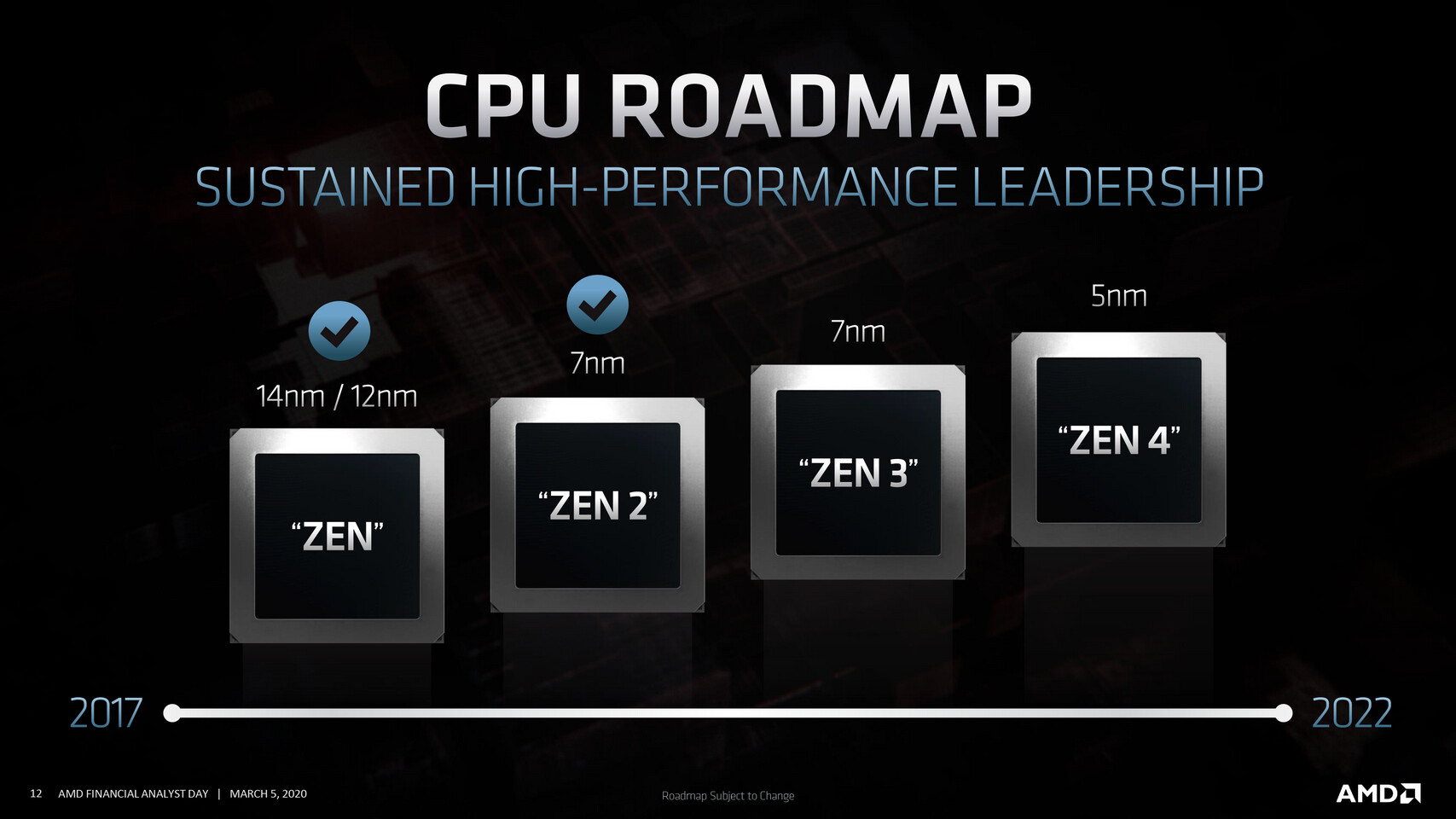
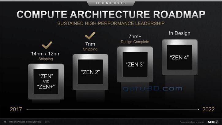
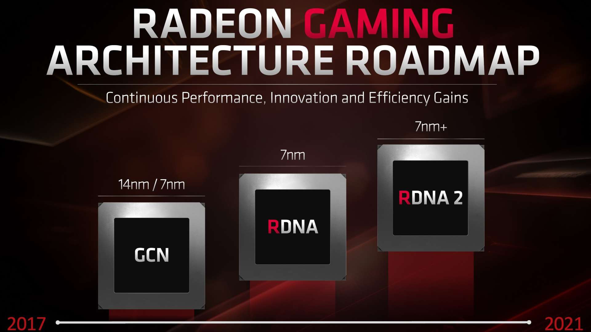
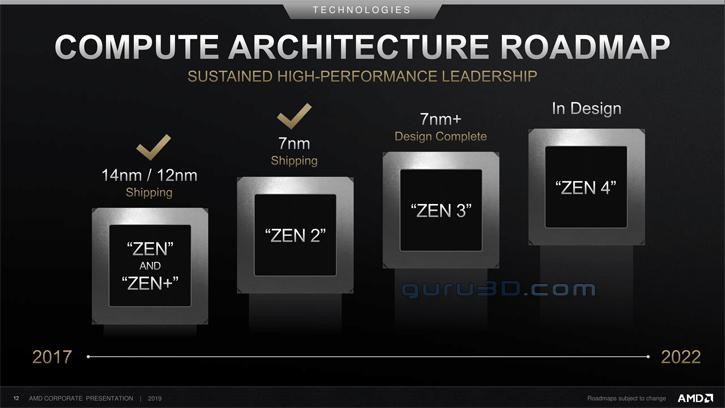
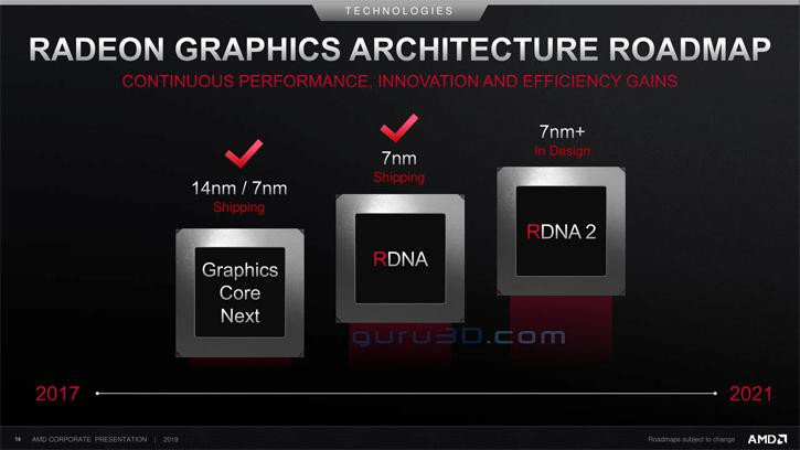
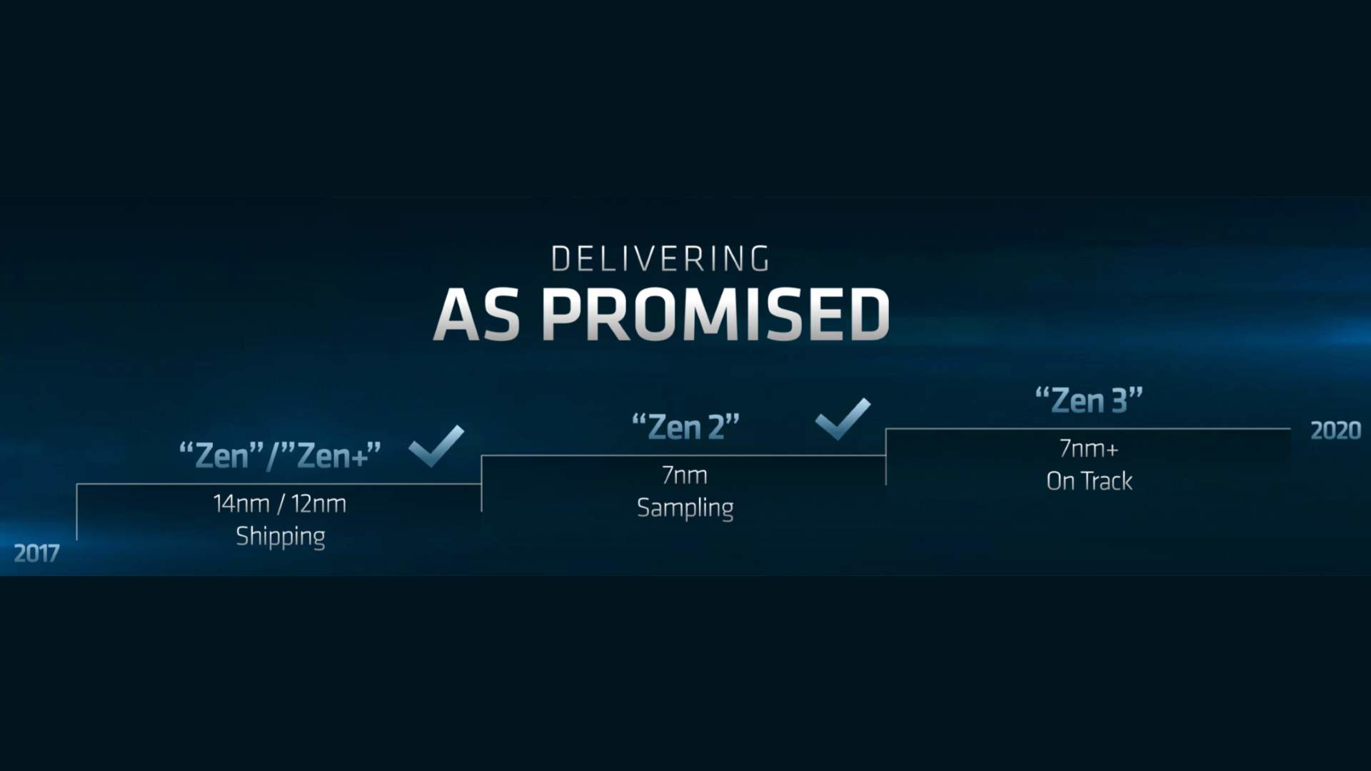
18:33 UTC: Looking forward, Lisa mentioned a few technology names without giving additional details: "... when you're talking about future cores, Zen 2, Zen 3, Zen 4, Zen 5, Navi, we're putting all of these architectures together, in new ways".

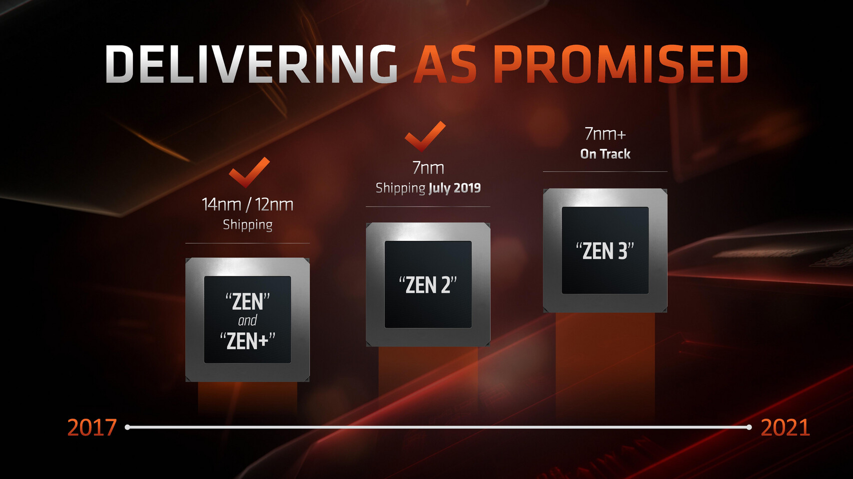
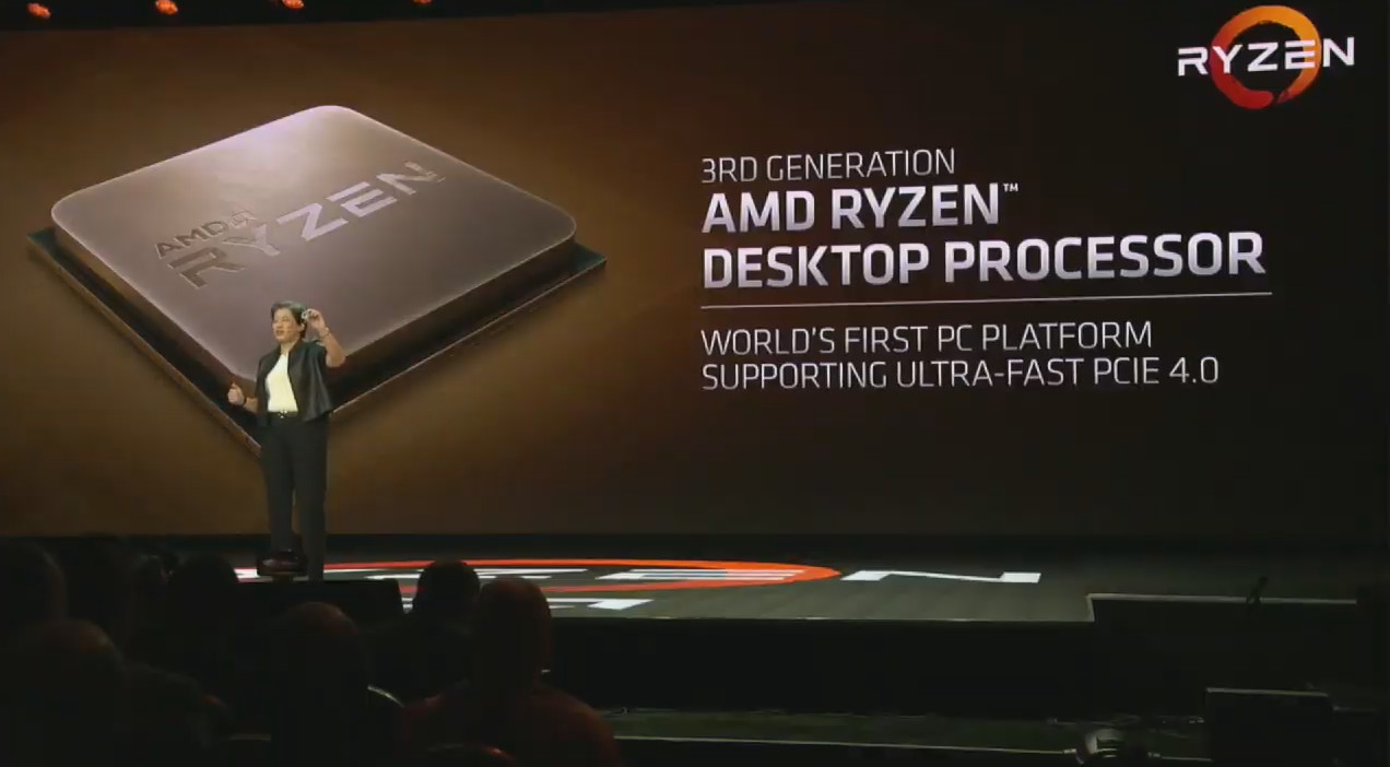
18:20 UTC: New Ryzen 3rd generation processors have been teased. The upcoming processors are based on Zen 2, using 7 nanometer technology. AMD showed a live demo of Forza Horizon 4, using Ryzen third generation, paired with Radeon Vega VII, which is running "consistently over 100 FPS at highest details at 1080p resolution". A second demo, using Cinebench, pitted an 8-core/16-thread Ryzen 3rd generation processor against the Intel Core i9-9900K. The Ryzen CPU was "not final frequency, an early sample". Ryzen achieved a score of 2057 using 135 W, while Intel achieved a score of 2040 using 180 W.. things are looking good for Ryzen 3rd generation indeed. Lisa also confirmed that next-gen Ryzen will support PCI-Express 4.0, which doubles the bandwidth per lane over PCI-Express 3.0. Ryzen third generation will run on the same AM4 infrastructure as current Ryzen; all existing users of Ryzen can simply upgrade to the new processors, when they launch in the middle of 2019 (we think Computex).
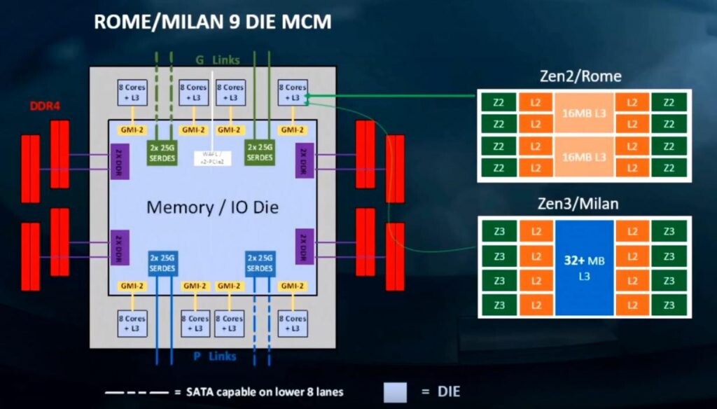
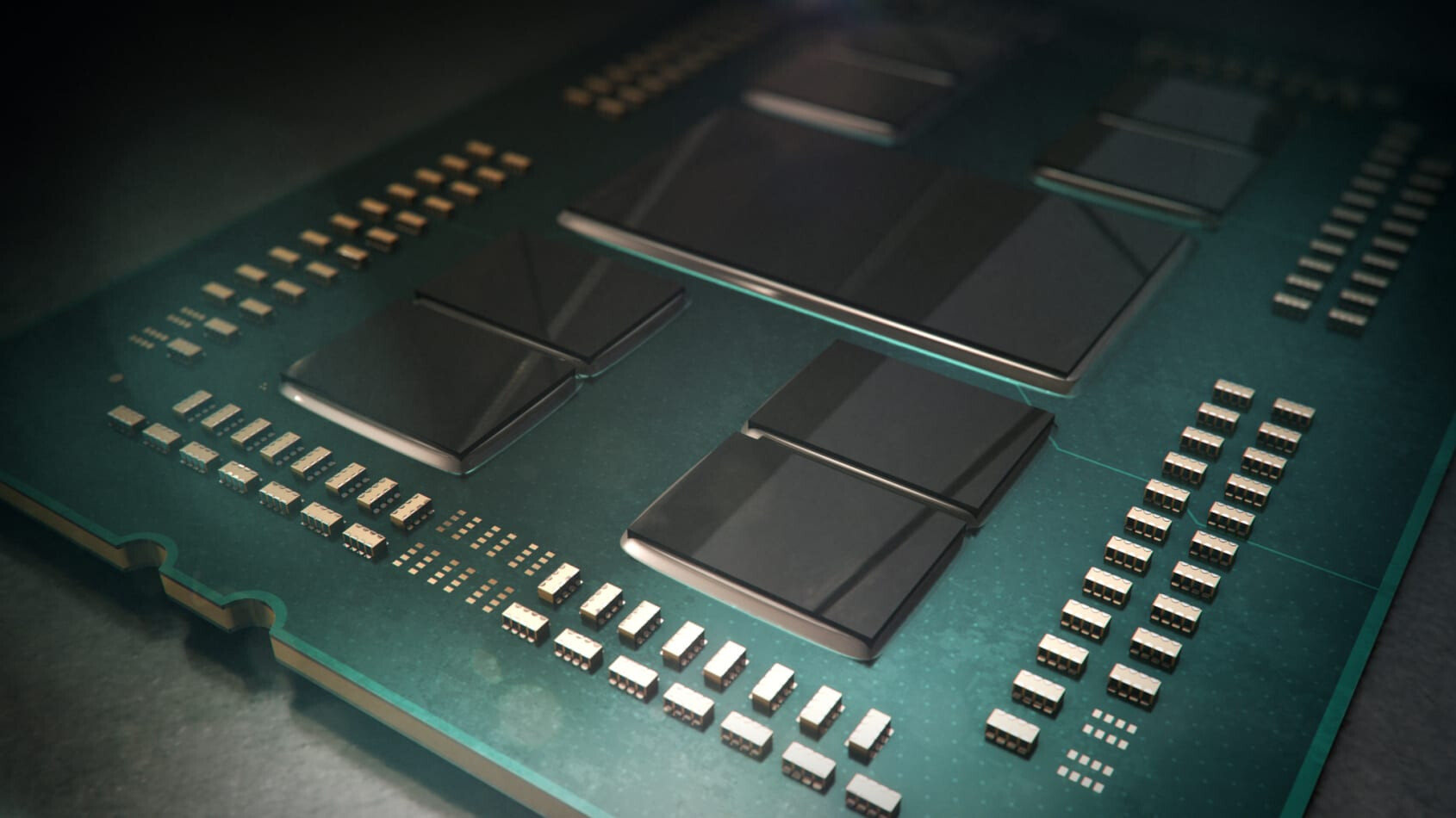
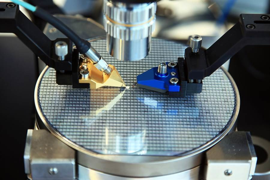
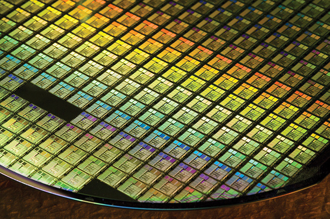
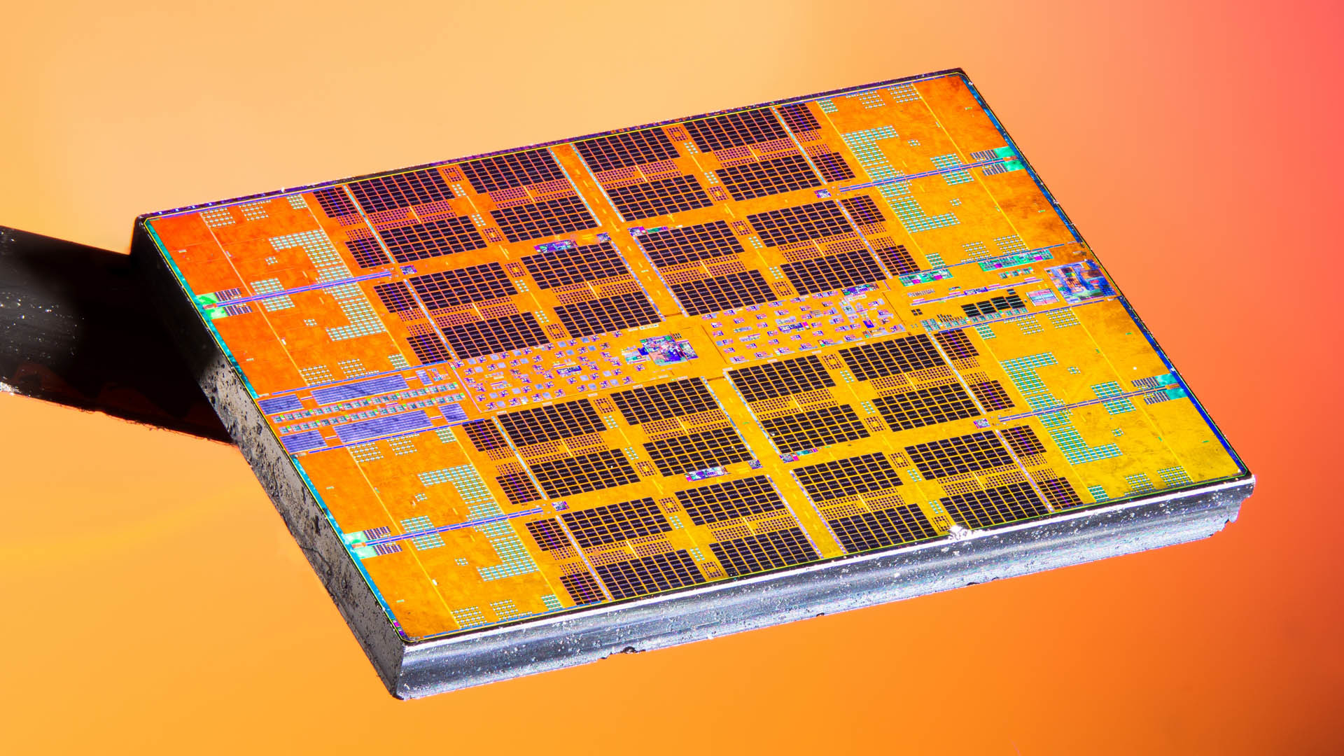
Ryzen third generation uses a chiplet design. The smaller die on the right contains 8-cores/16-threads using 7 nanometer technology. The larger die on the left is the IO die, which consists of things like the memory controller and PCI-Express connectivity, to shuffle data between the CPU core die and the rest of the system.

AMD Reveals CPU, Graphics 2018-2020 Roadmap at CES

AMD at CES shed some light on its 2018 roadmap, while taking the opportunity to further shed some light on its graphics and CPU projects up to 2020. Part of their 2018 roadmap was the company's already announced, across the board price-cuts for their first generation Ryzen processors. This move aims to increase competitiveness of its CPU offerings against rival Intel - thus taking advantage of the blue giant's currently weakened position due to the exploit saga we've been covering. This move should also enable inventory clearings of first-gen Ryzen processors - soon to be supplanted by the new Zen+ 12 nm offerings, which are expected to receive a 10% boost to power efficiency from the process shrink alone, while also including some specific improvements in optimizing their performance per watt profile. These are further bound to see their market introduction in March, and are already in the process of sampling.

On the CPU side, AMD's 2018 roadmap further points towards a Threadripper and Ryzen Pro refresh in the 2H 2018, likely in the same vein as their consumer CPUs that we just talked about. On the graphics side of their 2018 roadmap, AMD focused user's attention in the introduction of premium Vega offerings in the mobile space (with HBM2 memory integration on interposer, as well), which should enable the company to compete against NVIDIA in the discrete graphics space for mobile computers. Another very interesting tidbit announced by AMD is that they would be skipping the 12 nm process for their graphics products entirely; the company announced that it will begin sampling of 7 nm Vega products to its partners, but only on the Instinct product line of machine learning accelerators. We consumers will likely have to wait a little while longer until we see some 7 nm graphics cards from AMD.
Return to Keyword Browsing
May 15th, 2024 19:56 EDT change timezone

New Forum Posts

Popular Reviews

Controversial News Posts