News Posts matching #silicon manufacturing

Return to Keyword Browsing

Tenstorrent Selects Samsung Foundry to Manufacture Next-Generation AI Chiplet

Tenstorrent, a company that sells AI processors and licenses AI and RISC-V IP, announced today that it selected Samsung Foundry to bring Tenstorrent's next generation of AI chiplets to market. Tenstorrent builds powerful RISC-V CPU and AI acceleration chiplets, aiming to push the boundaries of compute in multiple industries such as data center, automotive and robotics. These chiplets are designed to deliver scalable power from milliwatts to megawatts, catering to a wide range of applications from edge devices to data centers.

To ensure the highest quality and cutting-edge manufacturing capabilities for its chiplet, Tenstorrent has selected Samsung's Foundry Design Service team, known for their expertise in silicon manufacturing. The chiplets will be manufactured using Samsung's state-of-the-art SF4X process, which boasts an impressive 4 nm architecture.

Samsung Preps Mass Production of Third-Generation 4 nm Chipsets, Start Date Expected Mid-2023

In a Samsung Electronics business report released on March 12, it was revealed that the giant electronics manufacturer will begin mass production of new chips through a 4 nm 2.3-generation process. The newly established manufacturing process is set to start by the end of H1 2023, which means that mid-June would be the expected commencement date. Samsung Semiconductor has managed to produce a satisfactory yield of wafers with the new generation chipsets.

Samsung Electronics has experienced significant problems with the production of previous generation 4 nm chips, and industry insiders have been surprised by the sudden announcement of the third generation version, given rumors pointing to the Hwaseong factory struggling to reach yields at the 60% mark. Qualcomm famously dropped Samsung in favor of TSMC as a source of 4 nm chipsets in 2022, due to disappointing yield figures.

US Strengthens China Export Bans, Limiting Access to Manufacturing Technology

The US Department of Commerce is in the process of increasing the stranglehold in tech exports directed to Chinese shores. The move is being made through the delivery of letters to US-based technology companies - namely KLA Corp, Lam Research Corp and Applied Materials Inc. - ordering them to stop the export of machines and equipment that can be used for sub-14 nm manufacturing. The move by the Department of Commerce only has validity for the companies that have been served by such a letter - at least until the Department codifies its newest regulations.

This means that only sellers with approved export licenses can keep doing business with Beijing, thus limiting the US companies China can work with as it aims to achieve at least a degree of self-sufficiency in the latest chipmaking tech. Perhaps the decision has come too late, however, as China's mainstay silicon manufacturing, SMIC, already manufactures chips at the 14 nm process (chips that have been deployed in China's Tinahu Light supercomputer already) and has even showcased manufacturing capability in the 7 nm field. It pays to remember that the US already had applied similar restrictions on equipment experts to China for the better part of two years - which apparently did little to stem China's capability to create increasingly denser semiconductor designs.

Intel Reveals Plans for US$20 Billion Chip Fab in Ohio

Rather unusually, Intel announced its latest chip fab plans not via a press release, but via an exclusive article in TIME magazine. It seems like an unusual strategy, as these kinds of things are normally not announced in this kind of fashion, especially as TIME doesn't exactly have close ties with Intel, nor the semiconductor industry as a whole, but maybe this is Intel's new way of trying to change the image of the company. Either which way, Intel is apparently planning on building no less than two fabs on the 1,000 acre (~4 square kilometer) site in New Albany, Ohio, which should be the workplace of some 3,000 people once it stands ready in 2025.

The article quotes Pat Gelsinger saying "Our expectation is that this becomes the largest silicon manufacturing location on the planet," as Intel has the option to double the land for its new fab site and apparently has plans for as many as eight fabs at the location. Additional fabs obviously depends on demand and crucially if Intel manages to full off its contract foundry business, since without it, it seems unlikely that Intel is going to need the additional six fabs in the foreseeable future, especially as Intel is in the final stages of finishing its new fab in Ireland, while also planning to announce a location for yet another fab somewhere in Europe and let's not forget Arizona. The TIME article goes into a lot more details as to what the new fabs mean for Ohio, but doesn't go into much more detail about Intel's plans for its future fabs there.

Update: Official press release below.

Samsung 5 nm Node Struggles With Yields, Reports Indicate Less Than 50% Yielding

Semiconductor manufacturing is no easy task. Every company in that business knows that, and the hardships of silicon manufacturing have been felt by even the greatest players like Samsung and Intel. Today, according to the latest report from Business Korea, Samsung is again in trouble with its 5 nm node. It has been reported previously that Samsung is struggling with yields of its 5 nm node, however, we didn't know just how much until now. According to the sources over at Business Korea, Samsung's 5 nm semiconductor node is experiencing less than 50% yields. That means, for example, that out of 100 chips manufactured on a single silicon wafer, only half are functional. And that is not good at all.

Usually, for a node to go into high-volume manufacturing (HVM), the yielding rate needs to be around 95%. In case it is not at that level, manufacturing of that node is not very efficient and not very profitable. The V1 Line in Hwaseong, where this Samsung 5 nm is made, uses EUV tools to manufacture the new node. While the yields are currently below 50%, it is expected to improve as Samsung engineers tweak and tune the node and the tools that are running the facility. We can expect to hear more about the yields of this node in the coming months.

UMC Investing $3.6 billion on 28 nm Manufacturing Capabilities Amidst Worldwide Semiconductor Shortages

UMC has announced plans to invest $3.6 billion in increasing output from its 28 nm manufacturing facilities. This move comes amidst a global semiconductor shortage, and isn't the first time a semiconductor manufacturer "dust off" their older manufacturing processes as a way to remove pressure from more modern silicon manufacturing capabilities. In this case, UMC will be increasing manufacturing output from its 300 mm Fab 12A facility in Tainan, Taiwan.

UMC has entered agreements with some of its clients, who will be paying upfront for expected chip rollout in the future. In exchange, clients will get the benefits of preset pricing (thus avoiding any potential increases arising from increased demand or general price fluctuation), as well as UMC's assurance of certain manufacturing volume allocation towards their needs. Fab 12A currently manufactures 90,000 300 mm wafers per month (wpm). An additional 10,000 wpm is being installed this year and phase six will add another 27,500 wpm to the mix. The mature 28 nm tools will be installed in floors that already feature support for future tooling upgrades to 14 nm. UMC expects to hire around 1,000 additional employees as part of this expansion effort.

Report: TSMC and UMC are Trucking in Water Amid Shortages

Manufacturing silicon is no easy task. You need to have all the right supplies available all the time. One of the most used ingredients in silicon manufacturing is water. Almost every process needs it and it needs to be constantly available to the manufacturer. According to the report coming from Reuters, Taiwan Semiconductor Manufacturing Company (TSMC) and United Microelectronics Corporation (UMC) are experiencing water shortages. The Taiwan island is in trouble, as the typhoon season has been rather mild and water supplies are at the historic lows. Water restrictions are in place all across the island and the reservoirs in the center and southern regions are at only 20% capacity.

The lack of water is a big problem for TSMC and UMC, as both companies rely on the constant income of it. With water restrictions in place, TSMC has to keep its facilities running and needs to solve the problem. That is why Taiwan's biggest silicon manufacturer is now making small orders of waters, delivered by a truckload. TSMC expects to compensate for the lack of water coming from its regular sources with truckloads of it. While we do not know the numbers of it, we can expect the water use to be very high if we take into account the number of wafers TSMC produces at its facilities.

Samsung to Build $17 Billion Silicon Manufacturing Plant in the US by 2023

Samsung has been one of the world's biggest foundries and one of three big players still left in the leading-edge semiconductor process development and manufacturing. However, the Korean giant is always seeking ways to improve its offerings, especially for Western customers. Today, it is reported that Samsung has reportedly talked with regulators in Texas, New York, and Arizona about building a $17 billion silicon manufacturing facility in the United States. The supposed factory is going to be located near Austin, Texas, and is supposed to offer around 1800 jobs. If the deal is approved and Samsung manages to complete the project on time, the factory is supposed to start mass production in Q4 of 2023.

What process is Samsung going to manufacture in the new fab? Well, current speculations are pointing out to the 3 nm node, with Samsung's special GAAFET (Gate All Around FET) technology tied to the new node. The fab is also expected to make use of extreme ultraviolet (EUV) lithography for manufacturing. Samsung already has a facility in the US called S2, however, that will not be upgraded as it is still serving a lot of clients. Instead, the company will build new facilities to accommodate the demand for newer nodes. It is important to note that Samsung will not do any R&D work in the new fab, and the company will only manufacture the silicon there.

AMD Reportedly in Plans to Outsource Partial Chip Production to Samsung

It's been doing the rounds in the rumor mill that AMD is looking to expand its semiconductor manufacturing partners beyond TSMC (for the 7 nm process and eventually 5 nm) and Global Foundries (12 nm process used in its I/O dies). The intention undoubtedly comes from the strain that's being placed on TSMC's production lines, as most foundry-less businesses outsource their wafer production to the Taiwanese companies' factories and manufacturing processes, which are currently the industry's best. However, as we've seen, TSMC is having a hard time scaling its production facilities to the unprecedented demand it's seeing from its consumers. The company also has recently announced it may prioritize new manufacturing capabilities for the automotive industry, which is also facing shortages in chips - and that certainly doesn't instill confidence in capacity increases for its non-automotive clients.

That's what originated form the rumor mill. Speculating, this could mean that AMD would be looking to outsource products with generally lower ASP to Samsung's foundries, instead of trying to cram even more silicon manufacturing onto TSMC's 7 nm process (where it already fabricates its Zen 3, RDNA 2, EPYC, and custom silicon solutions for latest-gen consoles). AMD might thus be planning on leveraging Samsung's 8 nm or even smaller fabrication processes as alternatives for, for example, lower-than-high-end graphics solutions and other product lines (such as APUs and FPGA production, should its acquisition of Xilinx come through).

TSMC to Roll Out 3nm Plus Manufacturing Process in 2023

The possibility barely exists to account for all the silicon manufacturing processes currently in development; TSMC themselves are rolling out 5 nm, 4 nm, 3 nm, and 2 nm processes at various points in time in the future. Now, the company has announced that it will be rolling out a revision of the 3 nm manufacturing process, named 3 nm Plus, come 2023. According to DigiTimes, the Taiwanese manufacturer's first client for this process will be Apple.

There is no information on what exactly 3 nm Plus leverages and offers over the "vanilla" 3 nm process. It could be anything from higher transistor density, lower power consumption, or higher operating frequency - or maybe a mixture of the three. The original 3 nm manufacturing process is set to offer a 15% performance gain over the current top-of-the-line 5 nm node, with 30% decreased power use and up to 70% density increase. Interestingly, TSMC is keeping their FinFet manufacturing technology, on grounds of better implementation costs and higher power efficiency compared to the more exotic GAA (Gate-All-Around) technology that its rival Samsung, for one, aims to implement in 3 nm.

China Develops Tools for 28 nm Silicon Manufacturing

When the US decided to impose sanctions on all US-made technology use in foreign countries (China), the Chinese semiconductor manufacturing industry seemed at the time that it would just completely stop. Without the tools to manufacture silicon, Chinese manufacturers would need to turn to other countries to search for a possible solution. That, however, turned out impossible as the US administration has decided to stop the silicon from going into the hands of Chinese companies, by making a condition that any US-made technology can not get to China. Many of the parts for silicon manufacturing are designed in the US, so they have the power to restrict the use.

Today, in a surprising turn of events, we have information that Shanghai Micro Electronic Equipment (SMEE) has developed a deep ultraviolet (DUV) lithography scanner that is set for delivery in 2021. With a plan to deliver it in the fourth quarter of 2021, SMEE has designed this DUV scanner for the production of 28 nm node. While not being the most advanced node available to date, it is a significant start for Chinese technology independence. ASML, the producer of such scanners, used to be one of the few options there, however, it just gained a competitor. China will deliver its new silicon on a 28 nm process at the end of 2021. Pictured below, you can see how the scanner from SMEE looks like.

TSMC Partners With Google and AMD to Push 3D Silicon

Silicon manufacturing is starting to get harder and harder every day, with new challenges appearing daily. It requires massive investment and massive knowledge to keep a silicon manufacturing company afloat. No company can survive that alone, so some collaborations are emerging. Today, thanks to the sources of Nikkei Asia, we have information that Taiwanese Semiconductor Manufacturing Company (TSMC) is collaborating with Google to push the production of 3D chip manufacturing process, that is said to overcome some of the silicon manufacturing difficulties. The sources also say that AMD is involved in the process as well, making Google and AMD the first customers of the advanced 3D chip design. The two companies are preparing designs for the new way of creating silicon and will help TSMC test and certify the process.

TSMC will deploy the 3D silicon manufacturing technology at its chip packaging plant in Miaoli, which is supposed to do mass production in 2022. With Google and AMD being the first customers of new 3D technology, it is exciting to see what new products will look like and how they will perform. The 3D approach is said to bring huge computing power increase, however, it is a waiting game now to see how it will look like.

Another Semiconductor Player Bites the Dust: Chinese HSMC Shutters Operations

The semiconductor manufacturing industry is a cutthroat competition mostly played between established forces. One need only look to AMD's decision to spin-off its manufacturing arm to create Global Foundries to see how even a grand company can hit manufacturing issues (though not only manufacturing issues hit AMD at that time, obviously) can threaten to shutter operations. Intel's recent issues with 10 nm and 7 nm fabrication also come to mind. as such, it comes at no great surprise that Chinese company Wuhan Hongxin Semiconductor Manufacturing Company (HSMC) has reportedly run out of cash. What's a little more surprising is how this company was actually backed by the Chinese government, and yet it still failed - proof of the semiconductor industry's technical and investment liquidity requirements.

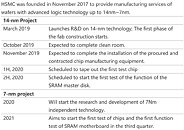
HSMC back in 2017 announced plans to bring online a manufacturing plant in the central Chinese province of Hubei. The aim was to manufacture 14 nm and 7 nm chips as early as 2019/2020, funded by a $20 billion loan and numerous funding rounds. HSMC's ex-CEO Chiang Shang-yi (who previously served as former head of R&D at TSMC) said to EETimes that "Investors ran short of cash." And that was it for the company's aspirations. The company has now been absorbed by the municipal government in the central Chinese province of Hubei, and what will come of that (and the company's future) remain uncertain.
Return to Keyword Browsing
May 31st, 2024 22:45 EDT change timezone

New Forum Posts

Popular Reviews

Controversial News Posts