Tuesday, July 6th 2021

Samsung 5 nm Node Struggles With Yields, Reports Indicate Less Than 50% Yielding

Semiconductor manufacturing is no easy task. Every company in that business knows that, and the hardships of silicon manufacturing have been felt by even the greatest players like Samsung and Intel. Today, according to the latest report from Business Korea, Samsung is again in trouble with its 5 nm node. It has been reported previously that Samsung is struggling with yields of its 5 nm node, however, we didn't know just how much until now. According to the sources over at Business Korea, Samsung's 5 nm semiconductor node is experiencing less than 50% yields. That means, for example, that out of 100 chips manufactured on a single silicon wafer, only half are functional. And that is not good at all.

Usually, for a node to go into high-volume manufacturing (HVM), the yielding rate needs to be around 95%. In case it is not at that level, manufacturing of that node is not very efficient and not very profitable. The V1 Line in Hwaseong, where this Samsung 5 nm is made, uses EUV tools to manufacture the new node. While the yields are currently below 50%, it is expected to improve as Samsung engineers tweak and tune the node and the tools that are running the facility. We can expect to hear more about the yields of this node in the coming months.
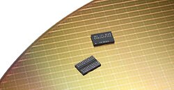
Sources: Business Korea, via HardwareLuxx
Add your own comment

16 Comments on Samsung 5 nm Node Struggles With Yields, Reports Indicate Less Than 50% Yielding

#1
TumbleGeorge
We are very close to end of easy performance increase just with using lower lithography node. Much better is to got more performance with better architecture. Clearly we need of new far far efficiency architectures, efficiency use all transistors and all of it's cycles and new priorities, not of 3nm...2nm...1nm...0nm...minus Xn pikometers.
Posted on Reply
#2
TheoneandonlyMrK
TumbleGeorgeWe are very close to end of easy performance increase just with using lower lithography node. Much better is to got more performance with better architecture. Clearly we need of new far far efficiency architectures, efficiency use all transistors and all of it's cycles and new priorities, not of 3nm...2nm...1nm...0nm...minus Xn pikometers.
There's easily ten to twenty more years of Node improvement and shrinking to go, 3Nm isn't a physically designated name, it's more of a product line name.
Posted on Reply
#3
Midland Dog
its less profitable to cancel the node than it is to sell it
Posted on Reply
#4
TheLostSwede
News Editor
TumbleGeorgeWe are very close to end of easy performance increase just with using lower lithography node. Much better is to got more performance with better architecture. Clearly we need of new far far efficiency architectures, efficiency use all transistors and all of it's cycles and new priorities, not of 3nm...2nm...1nm...0nm...minus Xn pikometers.
Hence why everyone's moving to "3D" stacked solutions, which Samsung recently delayed...
www.techpowerup.com/283983/samsung-3-nm-gaafet-node-delayed-to-2024
Posted on Reply
#5
Fourstaff
TSMC is still king after this, and it is getting hard to catch up to them.
Posted on Reply
#6
BorisDG
No wonder they are skipping their flagship Note 21 this year.
Posted on Reply
#7
ppn
5nm is not a full node. <20% area reduction VS 7nm, 6,5 and 4 are just different 7nm optimisations. in case of TSMC 5nm provides is full node 80% density vs 7nm or 133Mtr/mm² in case of apple M1. and 3nm is a whopping 70% density gain over 5nm. If nvidia released RTX 3090-GA102 on 7nm TSMC now it would fit in 420mm² 66Mtr/mm², the max size for EUV. But if 7nm (HP) Samsung is 77Mtr/mm² and 6nm is 10% better means ~~84. so not bad at all compared to TSMC's 7nm / 65.6 Mtr used in GA100.
Posted on Reply
#8
iO
Yield rate is useless without context.
50% YR would be horrible for something like Qualcomm's X60 at maybe ~30mm² but not too uncommon for some ~800mm² chip like next gens Nvidia Hopper.
Posted on Reply
#10
Tomorrow
ppn5nm is not a full node. <20% area reduction VS 7nm, 6,5 and 4 are just different 7nm optimisations. in case of TSMC 5nm provides is full node 80% density vs 7nm or 133Mtr/mm² in case of apple M1. and 3nm is a whopping 70% density gain over 5nm. If nvidia released RTX 3090-GA102 on 7nm TSMC now it would fit in 420mm² 66Mtr/mm², the max size for EUV. But if 7nm (HP) Samsung is 77Mtr/mm² and 6nm is 10% better means ~~84. so not bad at all compared to TSMC's 7nm / 65.6 Mtr used in GA100.
If Samsung has trouble with half-node then i dont even want to think about how absymal their full node yields would be.
Bad news for Nvidia i guess if they to stick with Samsung for 40 series.

Tho 30 series problems with efficiency stem from G6X more than they do from Samsung.
Posted on Reply
#11
TheLostSwede
News Editor
defaultluserBut compared to flash 3d stacking sram adds more cost.

I also don't think we are going to see mass-produced stackable DRAM anytime soon.
Oh, sure, it's not at all the same kind of stacking either. However, it's what the industry is moving towards and we'll most likely see the first products around 2025, assuming the foundry end works out.
Posted on Reply
#12
TheoneandonlyMrK
TheLostSwedeOh, sure, it's not at all the same kind of stacking either. However, it's what the industry is moving towards and we'll most likely see the first products around 2025, assuming the foundry end works out.
AMD announced stacked cache on they're 5### XT line.
Posted on Reply
#13
TheLostSwede
News Editor
TheoneandonlyMrKAMD announced stacked cache on they're 5### XT line.
Still not the same thing, but closer than NAND.
The stuff so far is layers of 2D transistors being stacked, but the future is "3D" transistors, i.e. not flat transistors.
They could in turn be used in layered stacks.
Apparently FinFET is considered a 3D transistor, so I guess in a sense, we're already there.
Posted on Reply
#14
yeeeeman
wait a minute....what do we expect from samsung to improve, since they have the 5nm process for what, more than a year, right?
Posted on Reply
#15
mtcn77
TheLostSwedeStill not the same thing, but closer than NAND.
The stuff so far is layers of 2D transistors being stacked, but the future is "3D" transistors, i.e. not flat transistors.
They could in turn be used in layered stacks.
Apparently FinFET is considered a 3D transistor, so I guess in a sense, we're already there.
This is 4D in that regard, the gate plane is crossing the source on 4 sides.
Posted on Reply
#16
Prima.Vera
Time to build those Chips on vertical (stacked layers), not just planar. "Terminator" movie gave some good ideas with cubical CPUs long time ago ;)
Posted on Reply
Add your own comment
Jun 3rd, 2024 09:28 EDT change timezone

New Forum Posts

Popular Reviews

Controversial News Posts