Saturday, March 16th 2013

Sapphire Radeon HD 7790 Dual-X Pictured, Tested
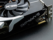
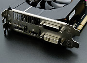
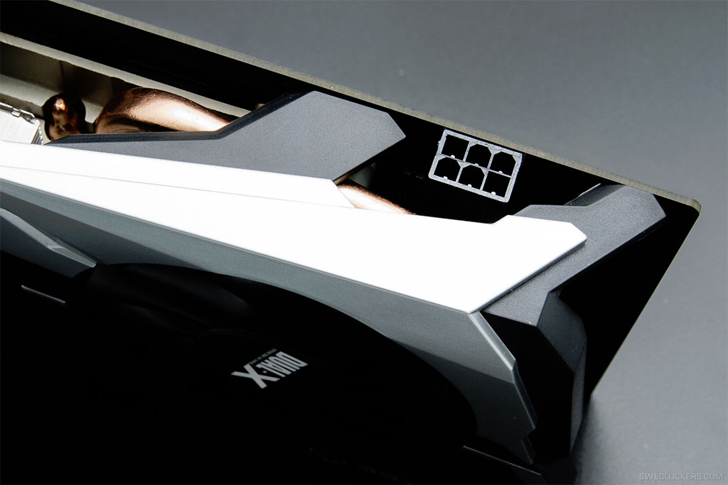
Here are the first pictures of Sapphire Radeon HD 7790 Dual-X, the company's premium offering based on AMD's new GPU. The card features Sapphire's in-house PCB and cooler designs, including an aluminium fin-stack heatsink ventilated by a pair of 80 mm fans, and a 21.5 cm long PCB. The card draws power from a single 6-pin PCIe power connector, its display outputs are similar to the HD 7850, with a pair of DVI connectors, HDMI, and DisplayPort. It can pair with another of its kind, only.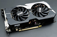
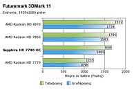
 SweClockers, who have one of these, wasted no time in putting it through 3DMark Fire Strike and 3DMark 11. In Fire Strike, the card scored 4026 points (graphics) compared to the 4395 points of Radeon HD 7850, which is just 8.3 percent slower. It's a similar story with 3DMark 11, where the HD 7790 scored 1583 points (graphics) compared to the 1734 points of HD 7850, just 8.7 percent slower. The reviewer is using a beta Catalyst driver bearing version number 12.101.2.0.
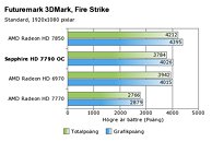
 A GPU-Z screenshot taken for the card reveals clock speeds of 1075 MHz core, and 1600 MHz memory, which results in a memory bandwidth of 102.4 GB/s. A point to note here is GPU-Z 0.6.8 doesn't officially support HD 7790 "Bonaire," and so some of the values which are not reported by the driver, such as stream processor count, TMU/ROP counts, and even memory bus width could be unreliably reported. Values such as clock speeds and memory size are driver-reported, and could be accurate.
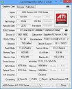
Source:
SweClockers


31 Comments on Sapphire Radeon HD 7790 Dual-X Pictured, Tested
Changes in memory bus width have never been a tried and true designator for a given class of cards.Given the 6970 was just a gelded 6850 (Barts with less Sp) AMD used the same PCB as a way of holding down cost, while able to raise core/memory clocks with the same power section. While no one can afford a more complex PCB it can be a big sales draw... As with what Nvidia intends with the alleged GTX 650 Boost. They look to run it on 192-bit to unbridle it from what they want you to believe is bandwidth starve 128-Bit. While is it just more a selling feature, than actually what a 768 Sp part can truly saturate?
I see it as GTX650 (GK107) has 2 SMX 128-Bit, while a GTX650Ti (GK106) has 3 SMX 128-bit and speeding the memory to 100Gb/s does assist about 10%. Then contemplate they provided a huge (68%) jump it bandwidth GTX660 (GK106) 5 SMX 192-Bit 144Gb/s, and between them there’s a jump (60%) in performance, but what's it from 2 extra SMX or bandwidth being used by those 2 extra SMX? While the GTX660Ti on GK104 with 7 SMX can do with 192-Bit. I just wonder will a 3 SMX part overwhelm anything much over 110Gb/s?
The numbering starts with architecture that sets different performance. Then to fill in gaps of performance they are forced to use other architectures because of design limitations. It's confusing when you know the technical details but to an average consumer who just want a performance metric then this makes logical sense.
Other than return shipping neither of the two cards I've had to return for manufacture warranty have cost me a cent (EVGA/PowerColor). Not sure where you live or why you'd have to spend $50 to get a direct replacement. While XFX not all their card will have Lifetime anymore only certain models provide that.