Thursday, June 15th 2017

Underside of AMD Ryzen Threadripper Pictured

AMD Ryzen Threadripper is a really big processor, and here's what its underside looks like. A multi-chip module (MCM) of two eight-core "Summit Ridge" dies, it is also AMD's first client-segment processor to feature a land-grid array (LGA) socket interface, since the decade-old Athlon64 FX 72; with the pins being located on the motherboard, and contact-points on the CPU package. Until now, AMD has limited large LGA sockets to its enterprise processors. The processor is based on the 4,094-pin socket SP3r2, which is increasingly being referred to by motherboard and cooler manufacturers as "TR4."

Given that it is an MCM of two dies, you can see a clear dividing line between two groups of the contact points that make up the total pin count of 4,094 pins. There are also two distinct ancillary cutouts which holds critical electrical components for the dies above. Something like this is lacking on the socket AM4 Ryzen "Summit Ridge" processors, where the cutout is blank, and the ancillaries are located around the CPU die, on the other side of the fiberglass substrate. AMD Ryzen Threadripper could be available from 27 July.
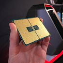
Source: Austin Evans (Twitter)
Add your own comment

34 Comments on Underside of AMD Ryzen Threadripper Pictured

#26
Scrizz
Live OR DieLol my point, LGA should be a standard by now but AMD still wants to use crap intel used for Pentium 1.
you mean Socket 478 used in the Northwood Pentium 4 era. ;)
Posted on Reply
#27
cdawall
where the hell are my stars
Live OR DieLol my point, LGA should be a standard by now but AMD still wants to use crap intel used for Pentium 1.
Name the benefits of LGA vs PGA. I'll wait.
Scrizzyou mean Socket 478 used in the Northwood Pentium 4 era. ;)
Later than that. Mobile chips were PGA right up until they went BGA.
Posted on Reply
#28
Frick
Fishfaced Nincompoop
I just miss the slot system.
Posted on Reply
#29
Scrizz
FrickI just miss the slot system.
I loved it on Pentium IIs and IIIs.

Nintendo had them too :laugh:
Posted on Reply
#30
Relayer
yogurt_21...wheres the pic of the amd exec making fun of kentsfield because it was two cpus slapped on the same die?

this looks like two cpus slapped together...
Over 10 years ago. How many CEO's ago was that for AMD? Different company today.
Posted on Reply
#31
Aquinus
Resident Wat-man
cdawallName the benefits of LGA vs PGA. I'll wait.
You should have read the thread, Holmes.
SteevoBiggest issue with LGA is the contact surface and how much power it can handle as pins get smaller, in a compressed pin and socket arrangement the contact area is much higher VS pins touching a surface.
Posted on Reply
#32
cdawall
where the hell are my stars
AquinusYou should have read the thread, Holmes.
That would be the opposite that is a benefit of PGA over LGA... Holmes.
Posted on Reply
#33
Aquinus
Resident Wat-man
cdawallThat would be the opposite that is a benefit of PGA over LGA... Holmes.
It's easier to fit more contacts in LGA and if the CPU costs more than the motherboard, a broken pin means replacing the cheaper component. Come on, you of all people should know this stuff and shouldn't need someone to validate it for you. I know that you know better. :p

Also, that was touched upon earlier as well.
Posted on Reply
#34
cdawall
where the hell are my stars
AquinusIt's easier to fit more contacts in LGA and if the CPU costs more than the motherboard, a broken pin means replacing the cheaper component. Come on, you of all people should know this stuff and shouldn't need someone to validate it for you. I know that you know better. :p

Also, that was touched upon earlier as well.
More like Intel doesn't have to replace the motherboard the manufacturer does. So more money for Intel.
Posted on Reply
Add your own comment
Nov 14th, 2024 09:19 EST change timezone

New Forum Posts

Popular Reviews

Controversial News Posts