6
Cores
12
Threads
15 W
TDP
3.5 GHz
Frequency
4.9 GHz
Boost
Phoenix
Codename
Socket FP8
Socket
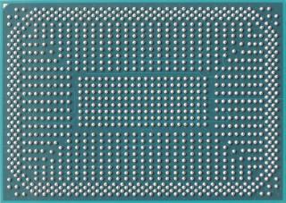
The AMD Ryzen 5 7640U is a mobile processor with 6 cores, launched in May 2023. It is part of the Ryzen 5 lineup, using the Zen 4 (Phoenix) architecture with Socket FP8. Thanks to AMD Simultaneous Multithreading (SMT) the core-count is effectively doubled, to 12 threads. Ryzen 5 7640U has 16 MB of L3 cache and operates at 3.5 GHz by default, but can boost up to 4.9 GHz, depending on the workload. AMD is building the Ryzen 5 7640U on a 4 nm production process using 25,000 million transistors. The silicon die of the chip is not fabricated at AMD, but at the foundry of TSMC. The multiplier is locked on Ryzen 5 7640U, which limits its overclocking capabilities.
With a TDP of 15 W, the Ryzen 5 7640U consumes very little energy. AMD's processor supports DDR5 memory with a dual-channel interface. The highest officially supported memory speed is 5600 MT/s, but with overclocking (and the right memory modules) you can go even higher. ECC memory is supported, too, which is an important capability for mission-critical systems, to avoid data corruption. For communication with other components in the system, Ryzen 5 7640U uses a PCI-Express Gen 4 connection. This processor features the Radeon 760M integrated graphics solution.
Hardware virtualization is available on the Ryzen 5 7640U, which greatly improves virtual machine performance. Programs using Advanced Vector Extensions (AVX) will run on this processor, boosting performance for calculation-heavy applications. Besides AVX, AMD has added support for the newer AVX2 and AVX-512 instructions, too.
Physical
| Socket: | AMD Socket FP8 |
|---|---|
| Foundry: | TSMC |
| Process Size: | 4 nm |
| Transistors: | 25,000 million |
| Die Size: | 178 mm² |
| Package: | FP8, FP7, FP7r2 |
| tJMax: | 100°C |
Processor
| Market: | Mobile |
|---|---|
| Production Status: | Active |
| Release Date: | May 3rd, 2023 |
| Part#: | 100-000001106 (FP7r2) 100-000001109 (FP7) 100-000001132 (FP8) |
Performance
| Frequency: | 3.5 GHz |
|---|---|
| Turbo Clock: | up to 4.9 GHz |
| Base Clock: | 100 MHz |
| Multiplier: | 35.0x |
| Multiplier Unlocked: | No |
| TDP: | 15 W |
| Configurable TDP: | 28 W |
Architecture
| Codename: | Phoenix |
|---|---|
| Generation: |
Ryzen 5
(Zen 4 (Phoenix)) |
| Memory Support: | DDR5 |
| LPDDR5x Speed: | 7500 MT/s |
| Rated Speed: | 5600 MT/s |
| Memory Bus: | Dual-channel |
| ECC Memory: | Yes |
| PCI-Express: |
Gen 4, 20 Lanes (CPU only) |
Core Config
| # of Cores: | 6 |
|---|---|
| # of Threads: | 12 |
| SMP # CPUs: | 1 |
| Integrated Graphics: | Radeon 760M |
Cache
| Cache L1: | 64 KB (per core) |
|---|---|
| Cache L2: | 1 MB (per core) |
| Cache L3: | 16 MB (shared) |
Features
|
Notes
| Graphics engine boost clock: 2600MHz |
Nov 13th, 2024 23:24 EST
change timezone
Latest GPU Drivers
New Forum Posts
- offset 240 to 280mm fan adapter (1)
- Board Power Limit (7)
- gpu always clocks at 300mhz (25)
- Awesome semi-open itx case&build showoff (0)
- TPU's Nostalgic Hardware Club (19382)
- NVIDIA App (18)
- Cryptocoin Value and Market Trend Discussion (1545)
- The Official Linux/Unix Desktop Screenshots Megathread (749)
- [INTEL]-How To Update Your Microcode for Intel HX 13/14th Gen. CPUs Laptops/Mobile Easily. (105)
- Got an Asus X870E-E Strix board for the extra M.2 cooling & extra slot... issues abound. (16)
Popular Reviews
- NVIDIA App v1.0 Review
- AMD Ryzen 7 9800X3D Review - The Best Gaming Processor
- Team Group A440 Lite 2 TB Review
- Glorious Series 2 Pro Wireless Review
- XPG Invader X Mini Review
- MIRPH-1 Open-Back Dynamic Driver Headphones Review
- Upcoming Hardware Launches 2024 (Updated Nov 2024)
- FiiO Industrial Park/Factory Tour + Interview with Founder
- DDR5 Memory Performance Scaling with AMD Zen 5
- Beelink GTi12 Ultra Mini-PC + EX Dock (Intel Core i9-12900H) Review
Controversial News Posts
- AMD Falling Behind: Radeon dGPUs Absent from Steam's Top 20 (222)
- AMD Ryzen 7 9800X3D Stocks Vaporized in Retail, Being Scalped (148)
- Quick Denuvo DRM Cracks Cost Game Publishers 20% in Revenue, According to Study (136)
- AMD Introduces Next-Generation AMD Ryzen 7 9800X3D Processor, $479, Nov 7 (124)
- Apple and Samsung in the Fray to Acquire Intel: Rumor (123)
- AMD Ryzen 7 9800X3D Comes with 120W TDP, 5.20 GHz Boost, All Specs Leaked (120)
- Microsoft Offers $30 Windows 10 Security Extension for Home Users (118)
- AMD Ryzen 7 9800X3D Has the CCD on Top of the 3D V-cache Die, Not Under it (110)


