6
Cores
12
Threads
28 W
TDP
3.5 GHz
Frequency
4.9 GHz
Boost
Hawk Point
Codename
Socket FP8
Socket
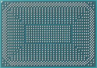
The AMD Ryzen Embedded 8640U is a mobile processor with 6 cores, launched in April 2024. It is part of the Ryzen Embedded lineup, using the Zen 4 (Hawk Point) architecture with Socket FP8. Thanks to AMD Simultaneous Multithreading (SMT) the core-count is effectively doubled, to 12 threads. Ryzen Embedded 8640U has 16 MB of L3 cache and operates at 3.5 GHz by default, but can boost up to 4.9 GHz, depending on the workload. AMD is building the Ryzen Embedded 8640U on a 4 nm production process using 25,000 million transistors. The silicon die of the chip is not fabricated at AMD, but at the foundry of TSMC. The multiplier is locked on Ryzen Embedded 8640U, which limits its overclocking capabilities.
With a TDP of 28 W, the Ryzen Embedded 8640U consumes only little energy. AMD's processor supports DDR5 memory with a dual-channel interface. The highest officially supported memory speed is 5600 MT/s, but with overclocking (and the right memory modules) you can go even higher. ECC memory is supported, too, which is an important capability for mission-critical systems, to avoid data corruption. For communication with other components in the machine, Ryzen Embedded 8640U uses a PCI-Express Gen 4 connection. This processor features the Radeon 760M integrated graphics solution.
Hardware virtualization is available on the Ryzen Embedded 8640U, which greatly improves virtual machine performance. Programs using Advanced Vector Extensions (AVX) will run on this processor, boosting performance for calculation-heavy applications. Besides AVX, AMD has added support for the newer AVX2 and AVX-512 instructions, too.
Physical
| Socket: | AMD Socket FP8 |
|---|---|
| Foundry: | TSMC |
| Process Size: | 4 nm |
| Transistors: | 25,000 million |
| Die Size: | 178 mm² |
| Package: | FP8, FP7, FP7r2 |
| tJMax: | 100°C |
Processor
| Market: | Mobile |
|---|---|
| Production Status: | Active |
| Release Date: | Apr 2nd, 2024 |
| Part#: | unknown |
Performance
| Frequency: | 3.5 GHz |
|---|---|
| Turbo Clock: | up to 4.9 GHz |
| Base Clock: | 100 MHz |
| Multiplier: | 35.0x |
| Multiplier Unlocked: | No |
| XDNA NPU: | 16 TOPS |
| TDP: | 28 W |
| Configurable TDP: | 15-30 W |
Architecture
| Codename: | Hawk Point |
|---|---|
| Generation: |
Ryzen Embedded
(Zen 4 (Hawk Point)) |
| Memory Support: | DDR5 |
| LPDDR5x Speed: | 7500 MT/s |
| Rated Speed: | 5600 MT/s |
| Memory Bus: | Dual-channel |
| ECC Memory: | Yes |
| PCI-Express: |
Gen 4, 20 Lanes (CPU only) |
Core Config
| # of Cores: | 6 |
|---|---|
| # of Threads: | 12 |
| SMP # CPUs: | 1 |
| Integrated Graphics: | Radeon 760M |
Cache
| Cache L1: | 64 KB (per core) |
|---|---|
| Cache L2: | 1 MB (per core) |
| Cache L3: | 16 MB (shared) |
Features
|
Notes
| Graphics engine boost clock: 2600MHz |
Nov 13th, 2024 23:26 EST
change timezone
Latest GPU Drivers
New Forum Posts
- offset 240 to 280mm fan adapter (1)
- Board Power Limit (7)
- gpu always clocks at 300mhz (25)
- Awesome semi-open itx case&build showoff (0)
- TPU's Nostalgic Hardware Club (19382)
- NVIDIA App (18)
- Cryptocoin Value and Market Trend Discussion (1545)
- The Official Linux/Unix Desktop Screenshots Megathread (749)
- [INTEL]-How To Update Your Microcode for Intel HX 13/14th Gen. CPUs Laptops/Mobile Easily. (105)
- Got an Asus X870E-E Strix board for the extra M.2 cooling & extra slot... issues abound. (16)
Popular Reviews
- NVIDIA App v1.0 Review
- AMD Ryzen 7 9800X3D Review - The Best Gaming Processor
- Team Group A440 Lite 2 TB Review
- Glorious Series 2 Pro Wireless Review
- XPG Invader X Mini Review
- MIRPH-1 Open-Back Dynamic Driver Headphones Review
- Upcoming Hardware Launches 2024 (Updated Nov 2024)
- FiiO Industrial Park/Factory Tour + Interview with Founder
- DDR5 Memory Performance Scaling with AMD Zen 5
- Beelink GTi12 Ultra Mini-PC + EX Dock (Intel Core i9-12900H) Review
Controversial News Posts
- AMD Falling Behind: Radeon dGPUs Absent from Steam's Top 20 (222)
- AMD Ryzen 7 9800X3D Stocks Vaporized in Retail, Being Scalped (148)
- Quick Denuvo DRM Cracks Cost Game Publishers 20% in Revenue, According to Study (136)
- AMD Introduces Next-Generation AMD Ryzen 7 9800X3D Processor, $479, Nov 7 (124)
- Apple and Samsung in the Fray to Acquire Intel: Rumor (123)
- AMD Ryzen 7 9800X3D Comes with 120W TDP, 5.20 GHz Boost, All Specs Leaked (120)
- Microsoft Offers $30 Windows 10 Security Extension for Home Users (118)
- AMD Ryzen 7 9800X3D Has the CCD on Top of the 3D V-cache Die, Not Under it (110)


