1
Cores
1
Threads
50 W
TDP
1467 MHz
Frequency
N/A
Boost
Thoroughbred
Codename
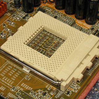
Socket A
Socket
The AMD Athlon XP 1700+ was a desktop processor with 1 core, launched in June 2002. It is part of the Athlon XP lineup, using the Thoroughbred-B architecture with Socket A. Athlon XP 1700+ has 256 KB of L2 cache and operates at 1467 MHz. AMD is making the Athlon XP 1700+ on a 130 nm production node using 37 million transistors. The multiplier is locked on Athlon XP 1700+, which limits its overclocking potential.
With a TDP of 50 W, the Athlon XP 1700+ consumes typical power levels for a modern PC. AMD's processor supports DDR1 memory. The highest officially supported memory speed is 400 MT/s, but with overclocking (and the right memory modules) you can go even higher. Although the processor doesn't come with integrated graphics, certain motherboards with compatible chipsets can provide this capability.
Many games will refuse to start on this processor due to the lack of the SSE2/SSE3/SSE4 instruction set.
Physical
| Socket: | AMD Socket A |
|---|---|
| Process Size: | 130 nm |
| Transistors: | 37 million |
| Die Size: | 80 mm² |
| Package: | FC-PGA |
Processor
| Market: | Desktop |
|---|---|
| Production Status: | End-of-life |
| Release Date: | Jun 10th, 2002 |
| Part#: | AXDA1700DUT3C |
Performance
| Frequency: | 1467 MHz |
|---|---|
| Turbo Clock: | N/A |
| Base Clock: | 133 MHz |
| Multiplier: | 11.0x |
| Multiplier Unlocked: | No |
| Voltage: | 1.6 V |
| TDP: | 50 W |
Architecture
| Codename: | Thoroughbred |
|---|---|
| Generation: |
Athlon XP
(Thoroughbred-B) |
| Memory Support: | DDR1 |
| Rated Speed: | 400 MT/s |
| ECC Memory: | No |
| Chipsets: | VIA KT266, KT333, KT400, KT400A, KT600, KT880, KM400, KM400A, nForce2, nForce2 400, nForce2 Ultra, nForce2 Ultra 400, SiS 741, SiS 746, SiS 748 |
Core Config
| # of Cores: | 1 |
|---|---|
| # of Threads: | 1 |
| SMP # CPUs: | 1 |
| Integrated Graphics: | On certain motherboards (Chipset feature) |
Cache
| Cache L1: | 128 KB |
|---|---|
| Cache L2: | 256 KB |
Features
|
Feb 22nd, 2025 07:39 EST
change timezone
Latest GPU Drivers
New Forum Posts
- Nvidia's GPU market share hits 90% in Q4 2024 (gets closer to full monopoly) (479)
- Solidigm NVMe Custom Modded Driver for All NVMe Brands SSDs & Any NVMe SSDs (203)
- can you use 2 of the same model "centers" as 2.0 ? (1)
- Warning about DOCP (12)
- Is this thermal paste or phase change pad? (4)
- Windows 11 General Discussion (5688)
- It's happening again, melting 12v high pwr connectors (858)
- Bizarre issue (0)
- PC Turns Off Immediately After Pressing Power Button--Must be Held Down to Power On (2)
- Where did the 7900xtx go? (20)
Popular Reviews
- MSI GeForce RTX 5070 Ti Ventus 3X OC Review
- Gigabyte GeForce RTX 5090 Gaming OC Review
- Galax GeForce RTX 5070 Ti 1-Click OC White Review
- ASUS GeForce RTX 5070 Ti TUF OC Review
- Ducky One X Inductive Keyboard Review
- MSI GeForce RTX 5070 Ti Vanguard SOC Review
- MSI GeForce RTX 5070 Ti Gaming Trio OC+ Review
- darkFlash DY470 Review
- MSI MAG Z890 Tomahawk Wi-Fi Review
- Palit GeForce RTX 5070 Ti GameRock OC Review
Controversial News Posts
- NVIDIA GeForce RTX 5090 Spotted with Missing ROPs, NVIDIA Confirms the Issue, Multiple Vendors Affected, RTX 5070 Ti, Too (306)
- AMD Radeon 9070 XT Rumored to Outpace RTX 5070 Ti by Almost 15% (302)
- AMD Plans Aggressive Price Competition with Radeon RX 9000 Series (269)
- AMD is Taking Time with Radeon RX 9000 to Optimize Software and FSR 4 (256)
- AMD Radeon RX 9070 and 9070 XT Listed On Amazon - One Buyer Snags a Unit (247)
- Edward Snowden Lashes Out at NVIDIA Over GeForce RTX 50 Pricing And Value (241)
- AMD Denies Radeon RX 9070 XT $899 USD Starting Price Point Rumors (239)
- New Leak Reveals NVIDIA RTX 5080 Is Slower Than RTX 4090 (215)


