2
Cores
2
Threads
65 W
TDP
3.4 GHz
Frequency
3.6 GHz
Boost
Trinity
Codename
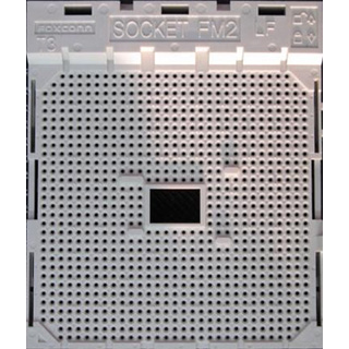
Socket FM2
Socket
The AMD A4-5300 was a desktop processor with 2 cores, launched in October 2012. It is part of the A4 lineup, using the Trinity architecture with Socket FM2. A4-5300 has 1 MB of L2 cache and operates at 3.4 GHz by default, but can boost up to 3.6 GHz, depending on the workload. AMD is building the A4-5300 on a 32 nm production process using 1,303 million transistors. The silicon die of the chip is not fabricated at AMD, but at the foundry of GlobalFoundries. The multiplier is locked on A4-5300, which limits its overclocking capabilities.
With a TDP of 65 W, the A4-5300 consumes typical power levels for a modern PC. AMD's processor supports DDR3 memory with a dual-channel interface. For communication with other components in the computer, A4-5300 uses a PCI-Express Gen 2 connection. This processor features the Radeon HD 7480D integrated graphics solution.
Hardware virtualization is available on the A4-5300, which greatly improves virtual machine performance. Programs using Advanced Vector Extensions (AVX) will run on this processor, boosting performance for calculation-heavy applications.
Physical
| Socket: | AMD Socket FM2 |
|---|---|
| Foundry: | GlobalFoundries |
| Process Size: | 32 nm |
| Transistors: | 1,303 million |
| Die Size: | 246 mm² |
| Package: | µPGA |
| tCaseMax: | 70°C |
Processor
| Market: | Desktop |
|---|---|
| Production Status: | End-of-life |
| Release Date: | Oct 2nd, 2012 |
| Part#: | AD5300OKA23HJ AD5300OKHJBOX |
Performance
| Frequency: | 3.4 GHz |
|---|---|
| Turbo Clock: | up to 3.6 GHz |
| Base Clock: | 100 MHz |
| Multiplier: | 36.0x |
| Multiplier Unlocked: | No |
| Voltage: | 1.475 V |
| TDP: | 65 W |
Architecture
| Codename: | Trinity |
|---|---|
| Generation: |
A4
(Trinity) |
| Memory Support: | DDR3 |
| Memory Bus: | Dual-channel |
| ECC Memory: | No |
| PCI-Express: | Gen 2 |
| Chipsets: | A88X, A85X, A78, A75, A68H, A55 |
Core Config
| # of Cores: | 2 |
|---|---|
| # of Threads: | 2 |
| SMP # CPUs: | 1 |
| Integrated Graphics: | Radeon HD 7480D |
Cache
| Cache L1: | 96 KB |
|---|---|
| Cache L2: | 1 MB (shared) |
Features
|
Notes
| 16KB L1 data cache per core. 64KB L1 instruction cache shared per two cores (per module). 1MB L2 cache shared per two cores (per module). 723MHz integrated graphics maximum core frequency. |
Feb 22nd, 2025 07:20 EST
change timezone
Latest GPU Drivers
New Forum Posts
- Nvidia's GPU market share hits 90% in Q4 2024 (gets closer to full monopoly) (476)
- Warning about DOCP (12)
- Is this thermal paste or phase change pad? (4)
- Windows 11 General Discussion (5688)
- It's happening again, melting 12v high pwr connectors (858)
- Bizarre issue (0)
- PC Turns Off Immediately After Pressing Power Button--Must be Held Down to Power On (2)
- Where did the 7900xtx go? (20)
- The Apocalypse is Near. (3)
- The TPU UK Clubhouse (25747)
Popular Reviews
- MSI GeForce RTX 5070 Ti Ventus 3X OC Review
- Gigabyte GeForce RTX 5090 Gaming OC Review
- Galax GeForce RTX 5070 Ti 1-Click OC White Review
- ASUS GeForce RTX 5070 Ti TUF OC Review
- Ducky One X Inductive Keyboard Review
- MSI GeForce RTX 5070 Ti Vanguard SOC Review
- MSI GeForce RTX 5070 Ti Gaming Trio OC+ Review
- darkFlash DY470 Review
- MSI MAG Z890 Tomahawk Wi-Fi Review
- Palit GeForce RTX 5070 Ti GameRock OC Review
Controversial News Posts
- NVIDIA GeForce RTX 5090 Spotted with Missing ROPs, NVIDIA Confirms the Issue, Multiple Vendors Affected, RTX 5070 Ti, Too (303)
- AMD Radeon 9070 XT Rumored to Outpace RTX 5070 Ti by Almost 15% (302)
- AMD Plans Aggressive Price Competition with Radeon RX 9000 Series (269)
- AMD is Taking Time with Radeon RX 9000 to Optimize Software and FSR 4 (256)
- AMD Radeon RX 9070 and 9070 XT Listed On Amazon - One Buyer Snags a Unit (247)
- Edward Snowden Lashes Out at NVIDIA Over GeForce RTX 50 Pricing And Value (241)
- AMD Denies Radeon RX 9070 XT $899 USD Starting Price Point Rumors (239)
- New Leak Reveals NVIDIA RTX 5080 Is Slower Than RTX 4090 (215)


