- Joined
- Oct 9, 2007
- Messages
- 47,244 (7.55/day)
- Location
- Hyderabad, India
| System Name | RBMK-1000 |
|---|---|
| Processor | AMD Ryzen 7 5700G |
| Motherboard | ASUS ROG Strix B450-E Gaming |
| Cooling | DeepCool Gammax L240 V2 |
| Memory | 2x 8GB G.Skill Sniper X |
| Video Card(s) | Palit GeForce RTX 2080 SUPER GameRock |
| Storage | Western Digital Black NVMe 512GB |
| Display(s) | BenQ 1440p 60 Hz 27-inch |
| Case | Corsair Carbide 100R |
| Audio Device(s) | ASUS SupremeFX S1220A |
| Power Supply | Cooler Master MWE Gold 650W |
| Mouse | ASUS ROG Strix Impact |
| Keyboard | Gamdias Hermes E2 |
| Software | Windows 11 Pro |
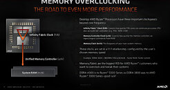
A leaked presentation slide by AMD for its Ryzen 5000 series "Zen 3" processors reveals details of the processor's memory interface. Much like the Ryzen 3000 series "Matisse," the Ryzen 5000 series "Vermeer" is a multi-chip module of up to 16 CPU cores spread across two 8-core CPU dies, and a unified I/O die that handles the processor's memory-, PCIe, and SoC interfaces. There are three configurable clock domains that ensure the CPU cores are fed with data at the right speed, and to ensure that the MCM design doesn't pose bottlenecks to the memory performance.
The first domain is fclk or Infinity Fabric clock. Each of the two CCDs (8-core CPU dies) has just one CCX (CPU core complex) with 8 cores, and hence the CCD's internal Infinity Fabric cedes relevance to the IFOP (Infinity Fabric over Package) interconnect that binds the two CCDs and the cIOD (client I/O controller die) together. The next frequency is uclk, or the internal frequency of the dual-channel DDR4 memory controller contained in the cIOD. And lastly, the mclk, or memory clock is the industry-standard DRAM frequency.

The three clock domains, according to AMD, are in a 1:1:1 synchrony, i.e. DRAM SDR clock is the same as uclk and fclk (for example, DDR4-3600 would see the memory real clock, uclk, and fclk run at 1800 MHz. AMD also appears to have increased the fclk limit to 2000 MHz with "Zen 3," so you can run memory clock at up to DDR4-4000 without having to engage the mclk:fclk 1:2 divider, which means DDR4-4000 on "Vermeer" will fetch as much of a real-world performance dividend as DDR4-3800 did for "Matisse." With AMD Ryzen, memory overclocking has been an effective way to improve overall system performance, due to the synchrony between mclk and fclk. and so, noticeable performance improvements can be had up to DDR4-4000, beyond which, you can still engage the divider to push mclk further up.
View at TechPowerUp Main Site
The first domain is fclk or Infinity Fabric clock. Each of the two CCDs (8-core CPU dies) has just one CCX (CPU core complex) with 8 cores, and hence the CCD's internal Infinity Fabric cedes relevance to the IFOP (Infinity Fabric over Package) interconnect that binds the two CCDs and the cIOD (client I/O controller die) together. The next frequency is uclk, or the internal frequency of the dual-channel DDR4 memory controller contained in the cIOD. And lastly, the mclk, or memory clock is the industry-standard DRAM frequency.

The three clock domains, according to AMD, are in a 1:1:1 synchrony, i.e. DRAM SDR clock is the same as uclk and fclk (for example, DDR4-3600 would see the memory real clock, uclk, and fclk run at 1800 MHz. AMD also appears to have increased the fclk limit to 2000 MHz with "Zen 3," so you can run memory clock at up to DDR4-4000 without having to engage the mclk:fclk 1:2 divider, which means DDR4-4000 on "Vermeer" will fetch as much of a real-world performance dividend as DDR4-3800 did for "Matisse." With AMD Ryzen, memory overclocking has been an effective way to improve overall system performance, due to the synchrony between mclk and fclk. and so, noticeable performance improvements can be had up to DDR4-4000, beyond which, you can still engage the divider to push mclk further up.
View at TechPowerUp Main Site


