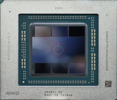
What is the chance that the GCD of Navi 31 is being made on the TSMC 3nm process, and not as claimed officially the 5nm process?
I found something in the data which doesn't add up.
Official data is:
Process Type N5 / N6 FinFET
Transistors 57,700 million
GCD Transistors 45,400 million
MCD Transistors 2,050 million x6
Density 109.1M / mm²
GCD Density 150.2 M / mm²
MCD Density 54.64 M / mm²
Die Size 529 mm²
GCD Die Size 304.35 mm²
MCD Die Size 37.52 mm² x6
6144 Cores, 384 TMUs, 192 ROPs

www.techpowerup.com
The thing is that there is no such high transistor density which can be achieved using the TSMC 5nm process - the maximum claimed is 138.2 MTr/mm²
https://en.wikipedia.org/wiki/5_nm_process
and 143.7 MTr/mm² on TSMC 4nm
https://en.wikipedia.org/wiki/5_nm_process
However, the TSMC 3nm process allows it - maximum is 224.2 MTr/mm² on N3P and N3X.
https://en.wikipedia.org/wiki/3_nm_process
I think GCD is made on 3nm process, while MCD is made on 7nm but extremely far from its potential maximum 114 MTr/mm².
To summarise.
GCD 150.2 MTr/mm²
TSMC 5nm process - maximum is 138.2 MTr/mm²
https://en.wikipedia.org/wiki/5_nm_process
TSMC 3nm process - maximum is 224.2 MTr/mm² (N3P | N3X)
https://en.wikipedia.org/wiki/3_nm_process
TSMC 7nm process - maximum is 114 MTr/mm²
https://en.wikipedia.org/wiki/7_nm_process
MCD 54.64 MTr/mm²
For a comparison, nvidia's AD102 transistor density is 125.3 M/mm², and offically claimed 4nm process - maximum is 143.7 M/mm².


