Raevenlord
News Editor
- Joined
- Aug 12, 2016
- Messages
- 3,755 (1.18/day)
- Location
- Portugal
| System Name | The Ryzening |
|---|---|
| Processor | AMD Ryzen 9 5900X |
| Motherboard | MSI X570 MAG TOMAHAWK |
| Cooling | Lian Li Galahad 360mm AIO |
| Memory | 32 GB G.Skill Trident Z F4-3733 (4x 8 GB) |
| Video Card(s) | Gigabyte RTX 3070 Ti |
| Storage | Boot: Transcend MTE220S 2TB, Kintson A2000 1TB, Seagate Firewolf Pro 14 TB |
| Display(s) | Acer Nitro VG270UP (1440p 144 Hz IPS) |
| Case | Lian Li O11DX Dynamic White |
| Audio Device(s) | iFi Audio Zen DAC |
| Power Supply | Seasonic Focus+ 750 W |
| Mouse | Cooler Master Masterkeys Lite L |
| Keyboard | Cooler Master Masterkeys Lite L |
| Software | Windows 10 x64 |
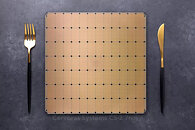
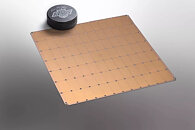
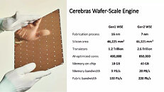
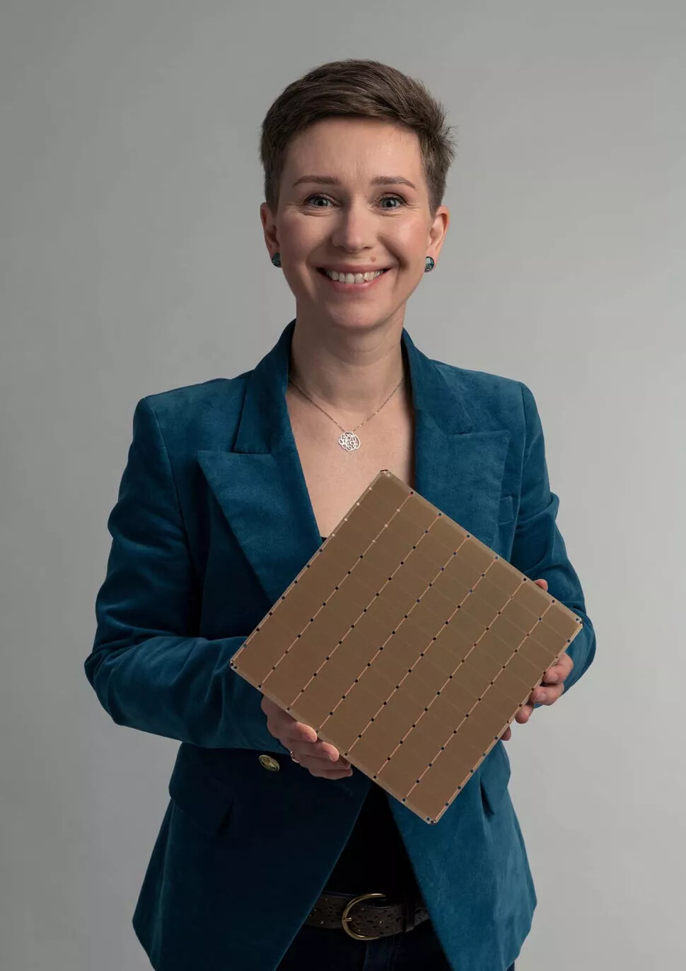
Cerebras has announced the successor to their record-breaking Wafer Scale Engine. The newly re-engineered Wafer Scale Engine 2 has been redesigned for TSMC's 7 nm manufacturing process - a severe improvement over the original's 16 nm. That Cerebras has moved on to TSMC's 7 nm for this giant, wafer-sized accelerator is telling of the confidence and state of yields on TSMC's 7 nm - if the process wasn't considered to be stable and guaranteeing incredibly good yields, I doubt such an effort would have been undertaken.

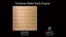
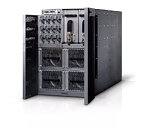
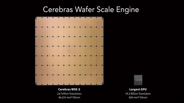
The updated Wafer Scale Engine 2 now packs a staggering 850,000 cores (compared to the original's 400,000); offers 40 GB of on-chip SRAM (up from 18 GB); 20 PetaBytes/s memory bandwidth (up from 9 PB/s), and 220 PB/s interconnect fabric speed (up from 100 PB/s). These improvements and increases have been achieved with the same power envelope as the original, set at a staggering 20 kW (system) and 15 kW (chip) power consumption. These are enabled by the much higher transistor density of 7 nm vs 16 nm, which enables 2.6 Trillion transistors on the Wafer Scale Engine 2 compared to a "paltry" 1.2 Trillion on the original, 16 nm version of it, whilst occupying the same 46,225 square millimeters (about 21.5 x 21.5 cm). Cerebras has one-upped itself, building upon what already had to be the most impressive feat of classical chip engineering.
View at TechPowerUp Main Site
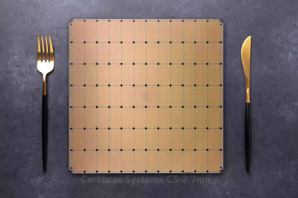
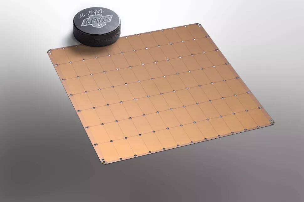
The updated Wafer Scale Engine 2 now packs a staggering 850,000 cores (compared to the original's 400,000); offers 40 GB of on-chip SRAM (up from 18 GB); 20 PetaBytes/s memory bandwidth (up from 9 PB/s), and 220 PB/s interconnect fabric speed (up from 100 PB/s). These improvements and increases have been achieved with the same power envelope as the original, set at a staggering 20 kW (system) and 15 kW (chip) power consumption. These are enabled by the much higher transistor density of 7 nm vs 16 nm, which enables 2.6 Trillion transistors on the Wafer Scale Engine 2 compared to a "paltry" 1.2 Trillion on the original, 16 nm version of it, whilst occupying the same 46,225 square millimeters (about 21.5 x 21.5 cm). Cerebras has one-upped itself, building upon what already had to be the most impressive feat of classical chip engineering.


View at TechPowerUp Main Site


