Report an Error


NVIDIA GeForce GT 710 PCIe x1
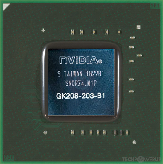
- Graphics Processor
- GK208B
- Cores
- 192
- TMUs
- 16
- ROPs
- 8
- Memory Size
- 1024 MB
- Memory Type
- DDR3
- Bus Width
- 64 bit
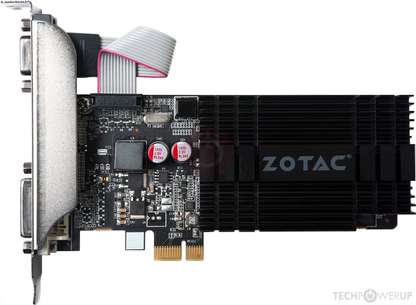
GPU

Rear

Back
Recommended Gaming Resolutions:
- 640x480
- 1280x720
- 1366x768
The GeForce GT 710 PCIe x1 was a graphics card by NVIDIA, launched on March 27th, 2014. Built on the 28 nm process, and based on the GK208B graphics processor, in its GK208-203-B1 variant, the card supports DirectX 12. Even though it supports DirectX 12, the feature level is only 11_0, which can be problematic with newer DirectX 12 titles. The GK208B graphics processor is a relatively small chip with a die area of only 87 mm² and 1,020 million transistors. Unlike the fully unlocked GeForce GT 730, which uses the same GPU but has all 384 shaders enabled, NVIDIA has disabled some shading units on the GeForce GT 710 PCIe x1 to reach the product's target shader count. It features 192 shading units, 16 texture mapping units, and 8 ROPs. NVIDIA has paired 1,024 MB DDR3 memory with the GeForce GT 710 PCIe x1, which are connected using a 64-bit memory interface. The GPU is operating at a frequency of 954 MHz, memory is running at 800 MHz.
Being a single-slot card, the NVIDIA GeForce GT 710 PCIe x1 does not require any additional power connector, its power draw is rated at 19 W maximum. Display outputs include: 1x DVI, 1x HDMI 1.4a, 1x VGA. GeForce GT 710 PCIe x1 is connected to the rest of the system using a PCI-Express 2.0 x1 interface. The card measures 146 mm in length, 112 mm in width, and features a single-slot cooling solution.
Being a single-slot card, the NVIDIA GeForce GT 710 PCIe x1 does not require any additional power connector, its power draw is rated at 19 W maximum. Display outputs include: 1x DVI, 1x HDMI 1.4a, 1x VGA. GeForce GT 710 PCIe x1 is connected to the rest of the system using a PCI-Express 2.0 x1 interface. The card measures 146 mm in length, 112 mm in width, and features a single-slot cooling solution.
Graphics Processor
- GPU Name
- GK208B
- GPU Variant
- GK208-203-B1
- Architecture
- Kepler 2.0
- Foundry
- TSMC
- Process Size
- 28 nm
- Transistors
- 1,020 million
- Density
- 11.7M / mm²
- Die Size
- 87 mm²
- Chip Package
- FCBGA-595
Graphics Card
- Release Date
- Mar 27th, 2014
- Generation
- GeForce 700
- Predecessor
- GeForce 600
- Successor
- GeForce 900
- Production
- End-of-life
- Bus Interface
- PCIe 2.0 x1
Clock Speeds
- GPU Clock
- 954 MHz
- Memory Clock
-
800 MHz
1600 Mbps effective
Memory
- Memory Size
- 1024 MB
- Memory Type
- DDR3
- Memory Bus
- 64 bit
- Bandwidth
- 12.80 GB/s
Render Config
- Shading Units
- 192
- TMUs
- 16
- ROPs
- 8
- SMX Count
- 1
- L1 Cache
- 16 KB (per SMX)
- L2 Cache
- 512 KB
Theoretical Performance
- Pixel Rate
- 3.816 GPixel/s
- Texture Rate
- 15.26 GTexel/s
- FP32 (float)
- 366.3 GFLOPS
- FP64 (double)
- 15.26 GFLOPS (1:24)
Board Design
- Slot Width
- Single-slot
- Length
- 146 mm
5.7 inches
- Width
- 112 mm
4.4 inches
- TDP
- 19 W
- Suggested PSU
- 200 W
- Outputs
- 1x DVI
1x HDMI 1.4a
1x VGA
- Power Connectors
- None
- Board Number
- P2132 SKU 14
Graphics Features
- DirectX
- 12 (11_0)
- OpenGL
- 4.6
- OpenCL
- 3.0
- Vulkan
- 1.2.175
- CUDA
- 3.5
- Shader Model
- 6.5 (5.1)
GK208B GPU Notes
| NVENC: NVDEC: 1st Gen PureVideo HD: VP5 VDPAU: Feature Set D L1 Cache is configurable from 16 KB up to 48 KB per SMX Latest Drivers: Windows XP / Server 2003 x64: GeForce Release 368.81 Quadro Release R319 U2 (321.01) Windows Vista: GeForce Release 365.19 Quadro Release R346 U7 (348.40) / R352 BETA (352.86) Windows 7 / 8 / 8.1 / 10 / 11 (x32 / x64): GeForce Release 391.35 / 474.89 Quadro Release R390 U9 (392.37) / R470 U16 (474.82) Quadro Mobile Release R390 U9 (392.37) / R418 U9 (426.78) |
Retail boards based on this design (1)
| Name | GPU Clock | Memory Clock | Other Changes |
|---|---|---|---|
| 954 MHz | 800 MHz |

Nov 19th, 2024 14:19 EST
change timezone
Latest GPU Drivers
New Forum Posts
- Glass mousepad (20)
- 3DMARK "LEGENDARY" (255)
- Got an Asus X870E-E Strix board for the extra M.2 cooling & extra slot... issues abound. (31)
- RX 580 2048SP Bios (2)
- Your PC ATM (35031)
- New Build (3)
- Gigabyte B550 x V2 - Game crashing (1)
- Is there a way to make web sites shut up about cookies? (18)
- The TPU UK Clubhouse (25315)
- Dell 7020 and 1660 super (2)
Popular Reviews
- NVIDIA SFF-Ready System Build & Benchmark Review - Build Small, Play Big
- AMD Ryzen 7 9800X3D Review - The Best Gaming Processor
- Quick Look: MOONDROP Quark2 Type-C In-Ear Monitors
- Valkyrie VK02 Lite Review
- Beelink GTi12 Ultra Mini-PC + EX Dock (Intel Core i9-12900H) Review
- Quick Look: Shanling M1 Plus Portable Audio Player
- NVIDIA App v1.0 Review
- Upcoming Hardware Launches 2024 (Updated Nov 2024)
- Epomaker TH40 Wireless Mechanical Keyboard Review
- Redragon K1NG 8K Review
Controversial News Posts
- AMD Falling Behind: Radeon dGPUs Absent from Steam's Top 20 (222)
- AMD Ryzen 7 9800X3D Stocks Vaporized in Retail, Being Scalped (152)
- AMD Introduces Next-Generation AMD Ryzen 7 9800X3D Processor, $479, Nov 7 (124)
- Apple and Samsung in the Fray to Acquire Intel: Rumor (123)
- AMD Ryzen 7 9800X3D Comes with 120W TDP, 5.20 GHz Boost, All Specs Leaked (120)
- Microsoft Offers $30 Windows 10 Security Extension for Home Users (118)
- AMD Ryzen 7 9800X3D Has the CCD on Top of the 3D V-cache Die, Not Under it (110)
- TechPowerUp is Hiring a Power Supply (PSU) Reviewer (105)