Report an Error
Intel Ironlake

Ironlake
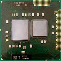
Intel's Ironlake GPU uses the Generation 5.75 architecture and is made using a 45 nm production process at Intel. With a die size of 114 mm² and a transistor count of 177 million it is a small chip. Ironlake supports DirectX 10.1. Modern GPU compute technologies are not available. It features 96 shading units, 16 texture mapping units and 2 ROPs.
Graphics Processor
- Released
- Jan 10th, 2010
- GPU Name
- Ironlake
- Architecture
- Generation 5.75
- Foundry
- Intel
- Process Size
- 45 nm
- Transistors
- 177 million
- Density
- 1.6M / mm²
- Die Size
- 114 mm²
Graphics Features
- DirectX
- 10.1
- OpenGL
- 2.1
- OpenCL
- N/A
- Vulkan
- N/A
- Shader Model
- 4.1
Render Config
- Shading Units
- 96
- TMUs
- 16
- ROPs
- 2
- Execution Units
- 16
- Max. TDP
- 35 W
All Generation 5.75 GPUs
- Intel Ironlake
Intel GPU Architecture History
- 2023 Xe-LPG
- 2022-2023 Generation 12.7
- 2021-2024 Generation 12.5
- 2021-2023 Generation 12.2
- 2020-2021 Generation 12.1
- 2019-2021 Generation 11.0
- 2016-2020 Generation 9.5
- 2015-2016 Generation 9.0
- 2014-2015 Generation 8.0
- 2013 Generation 7.5
- 2012-2013 Generation 7.0
- 2011 Generation 6.0
- 2010-2013 Knights
- 2010 Generation 5.75
- 2008-2010 PowerVR SGX545
- 2008 Generation 5.0
- 2008-2010 PowerVR SGX535
- 2006-2007 Generation 4.0
- 2005-2006 Generation 3.5
- 2004-2005 Generation 3.0
- 2002-2003 Generation 2.0
- 1998 i740
- 1998-2002 Generation 1.0
Graphics cards using the Intel Ironlake GPU
| Name | Chip | Memory | Shaders | TMUs | ROPs | Base Clock | Boost Clock | Memory Clock |
|---|---|---|---|---|---|---|---|---|
| System Shared | 96 | 16 | 2 | 133 MHz | 500 MHz | System Shared | ||
| System Shared | 96 | 12 | 2 | 533 MHz | System Shared |

Ironlake GPU Notes
| Arrandale Processors Clarkdale Processors |
Nov 19th, 2024 10:34 EST
change timezone
Latest GPU Drivers
New Forum Posts
- Share your AIDA 64 cache and memory benchmark here (2988)
- Technical Issues - TPU Main Site & Forum (2024) (380)
- The TPU UK Clubhouse (25311)
- Black monitor screen.. only sometimes. (13)
- Overclocking Gskill DDR5 6000 2x32(64gb) to 7000 CAS 30 (0)
- Inconsistent POSTing on PC ( already replaced multiple parts) (91)
- AMD RX 7000 series GPU Owners' Club (1247)
- Is there a way to make web sites shut up about cookies? (3)
- Your PC ATM (35028)
- Waterpik flosser faulty; On\Off button not working, low pressure, cannot change the speed (0)
Popular Reviews
- AMD Ryzen 7 9800X3D Review - The Best Gaming Processor
- NVIDIA SFF-Ready System Build & Benchmark Review - Build Small, Play Big
- Quick Look: MOONDROP Quark2 Type-C In-Ear Monitors
- Valkyrie VK02 Lite Review
- Beelink GTi12 Ultra Mini-PC + EX Dock (Intel Core i9-12900H) Review
- NVIDIA App v1.0 Review
- Quick Look: Shanling M1 Plus Portable Audio Player
- Epomaker TH40 Wireless Mechanical Keyboard Review
- Upcoming Hardware Launches 2024 (Updated Nov 2024)
- Redragon K1NG 8K Review
Controversial News Posts
- AMD Falling Behind: Radeon dGPUs Absent from Steam's Top 20 (222)
- AMD Ryzen 7 9800X3D Stocks Vaporized in Retail, Being Scalped (152)
- AMD Introduces Next-Generation AMD Ryzen 7 9800X3D Processor, $479, Nov 7 (124)
- Apple and Samsung in the Fray to Acquire Intel: Rumor (123)
- AMD Ryzen 7 9800X3D Comes with 120W TDP, 5.20 GHz Boost, All Specs Leaked (120)
- Microsoft Offers $30 Windows 10 Security Extension for Home Users (118)
- AMD Ryzen 7 9800X3D Has the CCD on Top of the 3D V-cache Die, Not Under it (110)
- TechPowerUp is Hiring a Power Supply (PSU) Reviewer (105)